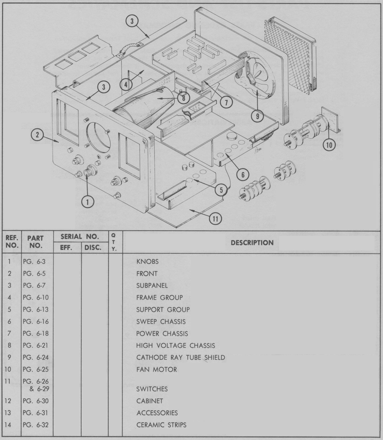
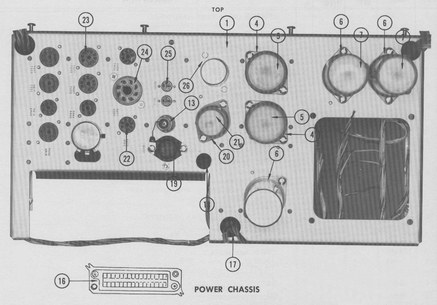
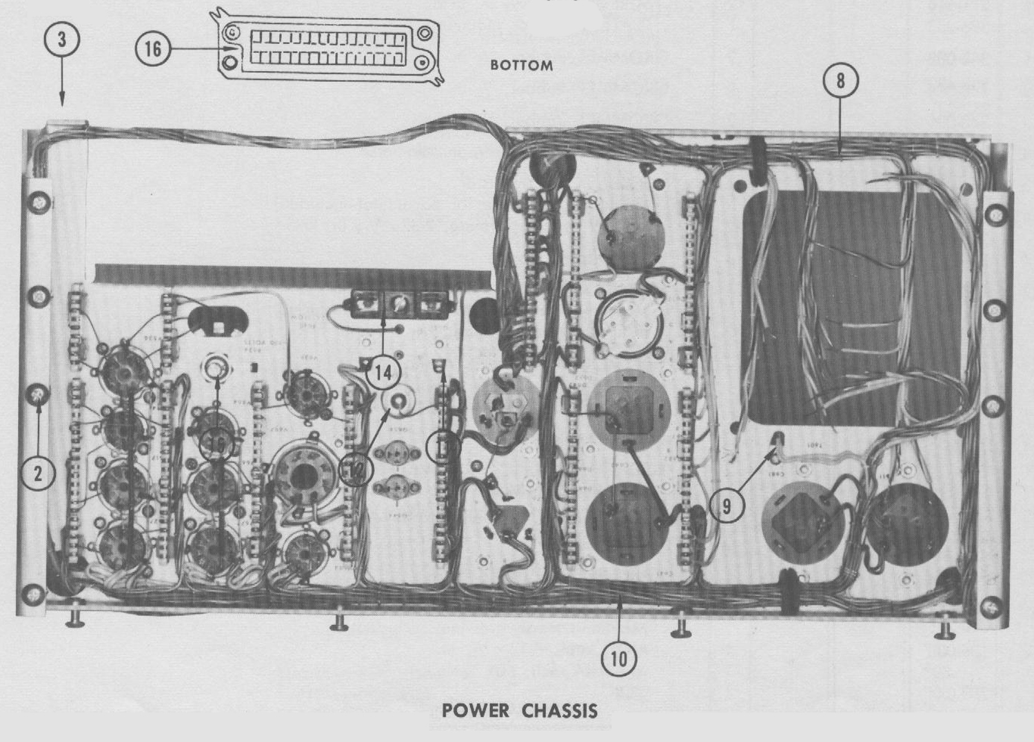
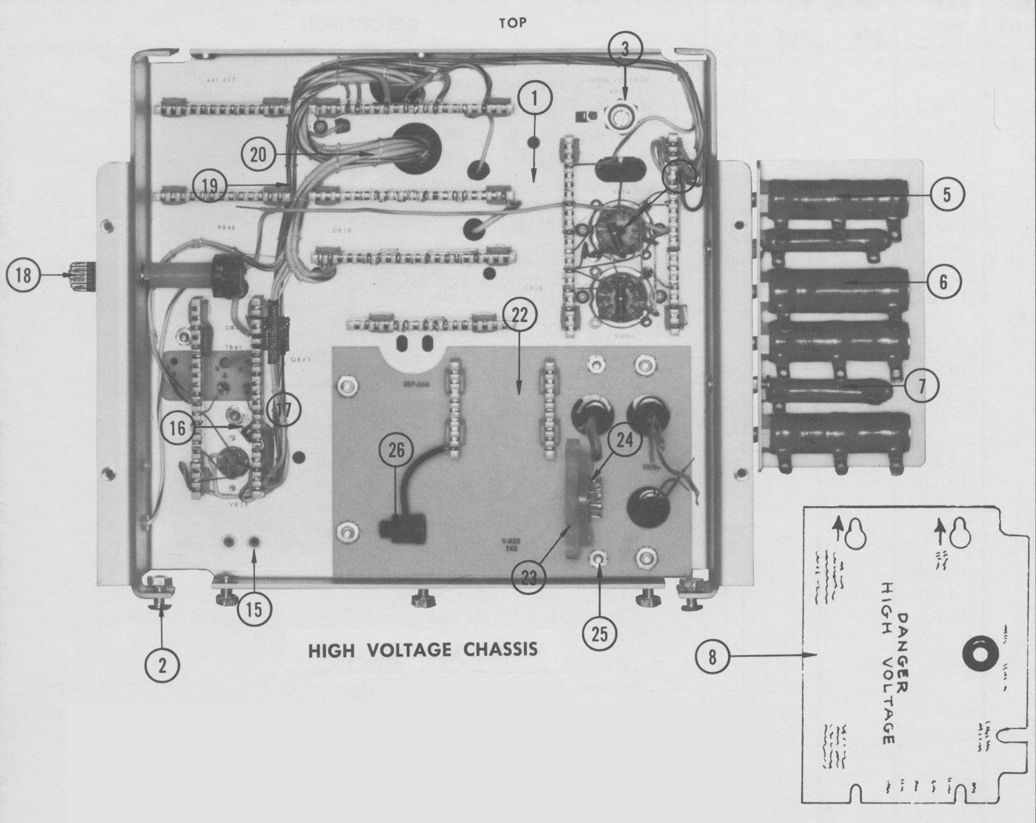
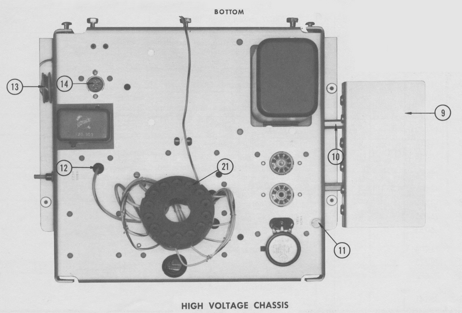
Oscilloscope Tektronix Type 565 serial 689, eighth part (MITI Museum)

Oscilloscopio Tektronix Type 565. Ottava parte.
Nell’inventario D del 1956 si trova al n° 3747 e risulta acquistato nell’agosto del 1964; vi si legge: “Silvestar ltd. Milano. Oscilloscopio Tektronix mod. 565 matr 689. Dest. Elettronica ₤ 1·678·600”. Insieme alla fotocamera che è al n° 3746, dove si legge: “Silvestar ltd. Milano. Macchina fotografica Tektronix mod. C-12 completa di Bezel-Tektronix. Dest. Elettronica. ₤ 557·700”.
Il testo continua dalla settima parte.
§§§

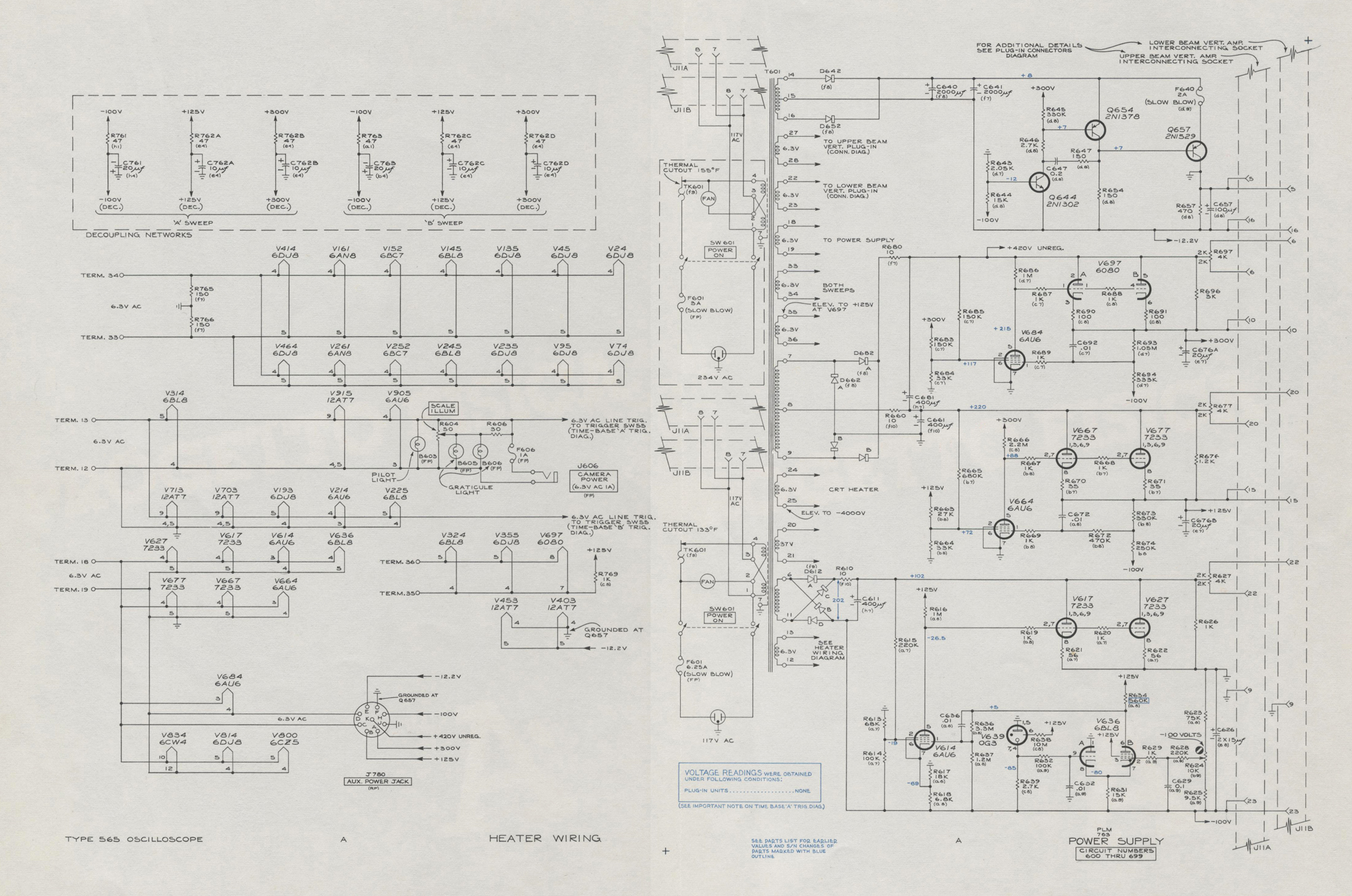
          «LOW VOLTAGE POWER SUPPLIES
General
The Low Voltage Power Supplies consist of four

interdependent, regulated voltage sources. Each supply is
capable of maintaining an accurate dc output voltage
having a low percentage of ripple, even though the
input line voltage and the output load may vary considerably.
-100 Volt Supply
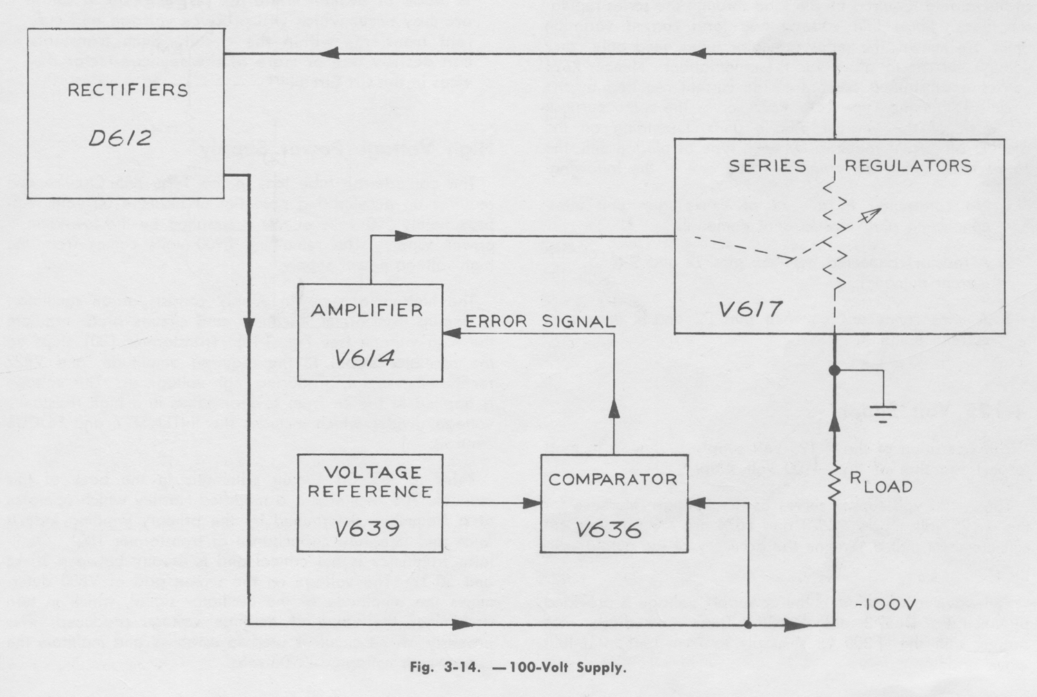
When the design-center voltage is applied to the primary
of T601, the voltage across secondary terminals 6 and 11 is
about 145 volts rms. This voltage is applied to a conventional
full-wave bridge rectifier, D612, producing about 200 volts dc across filter capacitor C611. This voltage is then divided between the load and the series regulator tubes.
The block diagram Fig. 3-14 shows the basic elements of the
circuit which accomplish this division.
The regulator tubes function as a variable resistor in
series with the load. In order to maintain a stable voltage
across the load, their plate resistance must be changed as
required to offset the effect of a change in line voltage or

load current. To accomplish this, the output voltage is
constantly compared to a fixed reference voltage by the
comparator V636. Any error thus detected is amplified and
applied to the series regulators. Their plate resistance is
thereby changed and the proper output voltage is restored.

Refer to the Power Supply schematic in the back of this
manual. The voltage reference tube V639 applies a stable
-85 volts to the ‘A’ grid of a long-tailed difference amplifier

V636. This establishes an essentially constant voltage at the
common cathodes of both V636A and V636B. A sample of
the supply output voltage is obtained from the -100 VOLTS
control, R624. (This sample will always be about -85 volts,
since it is the voltage actually being regulated to match the

reference voltage. Since the -100 VOLTS control is set so
the sample is 85% of the total voltage across R623, R624 and R625, the total voltage will also be regulated.) If a positive-going change occurs in the output voltage, the grid voltage on V636B changes in the positive direction. The current through V636B increases and its plate voltage drops. This negative-going voltage change is applied to the control grid of amplifier V614. The current through V614 decreases and its plate voltage rises, carrying the grids of V617 and V627 positive. The regulator tubes’ plate resistance decreases, therefore increasing the current through the load.
This results in an increased voltage drop across the load, thus offsetting the error.
Negative-going changes are corrected in the same way
except for error signal polarities. Due to the high gain of the
amplifier circuits and their ability to respond quickly, the
supply in effect corrects for changing line voltage and load
conditions before a significant change can occur in the
output voltage.
The dc voltage across C611 bears a substantial amount
of ripple. A sample of this ripple is applied to the screen
grid of V614. The screen grid acts as a second signal grid
and aids in eliminating much of the ripple from the supply
output. C636 and C629 also aid in eliminating ripple since

they offer less attenuation to ac error signals than do the
resistive voltage dividers. C626 lowers the supply output
impedance.
R626 and R627 are particularly important elements in
the -100 volt supply. It would be impractical to pass all
of the current required by the load through the series

regulator tubes.  Since line voltage and load current variationlimits are known, the series regulator tubes
need only carry enough current to allow for these variations. Hence, R626 carries a substantial amount of the current required by the circuits within the Type 565. R627 serves the same purpose for each of the vertical plug-in units. Depending on the amount of current required by each type of plug-in unit, the connections within the plug-in will be one of the following:
1.No connection to pin 22 of the plug-in unit
interconnecting plug (low current demand).
2.A resistor connected between pins 22 and 9 (moderate
current demand).
3.A wire connected between pins 22 and 9 (maximum
current demand).
+125 Volt Supply
The operation of the +125 volt supply is similar, in most
respects, to that of the -100 volt supply.
The -100 volt supply serves as the voltage reference for
the +125 volt supply. R673 and R674 are the principle
circuit elements that determine the accuracy of the output
voltage.
Full-wove rectification of the ac supply voltage is provided
by rectifiers D662A and D662B. These two diodes are
shared with the +300 volts supply to form half of a full-
wave bridge.
+300 Volt Supply
The only significant difference between the +125 and
+300 volt supplies is the +420 volt unregulated output

associated with the +300 volt supply. This voltage is used
in the oscillator portion of the Crt Circuit.
-12.2 Volt Supply
R643 and R644 provide the reference voltage at the base

of Q644. Any voltage error at the emitter of Q644 is
amplified, but not inverted, and applied to the base of Q654.
Q654 amplifies and inverts the error signal, providing the
necessary drive for the series regulator Q657. C647 and
R647 provide phase correction for Q654, thereby stabilizing
the regulator.
The -12.2 volt supply does not employ shunt resistors
as do the other three supplies. Instead, all load current
passes through the series regulator. Fuse F640 protects
Q657 from overload. C657 reduces the supply output
impedance.                           
CRT CIRCUIT
                              CAUTION
Always make or break voltmeter connections at

any of the high-voltage points in the Crt Circuit
(except for the HIGH VOLTAGE TEST POINT)
while the instrument is turned off. If a connection
is made or broken while the power is on, a small
arc may occur which will produce voltage and
current transients within the circuit. Such transients
can destroy one or more of the semiconductor
devices in the Crt Circuit.
High Voltage Power Supply
The cathode-ray tube (crt) in the Type 565 Oscilloscope

requires an accelerating potential of about 4100 volts.
Approximately 200 volts of this is supplied by the low-voltage power supply. The remaining 3900 volts comes from the high-voltage power supply.
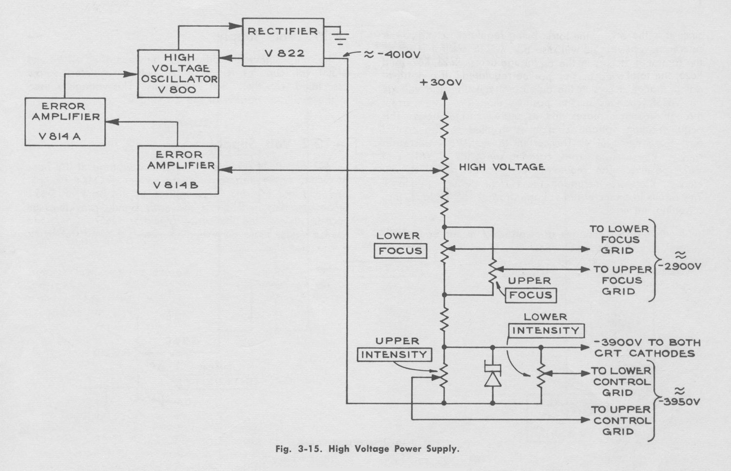
The high-voltage power supply consists of an oscillator,
a step-up transformer, rectifiers, and circuits which regulate
the high voltage (see Fig. 3-15). Transformer T801 steps up
the oscillator signal to the required amplitude, and V822
rectifies the signal, producing high voltage dc. This voltage
is applied to the crt from several points in a high resistance

voltage divider which includes the INTENSITY and FOCUS controls.
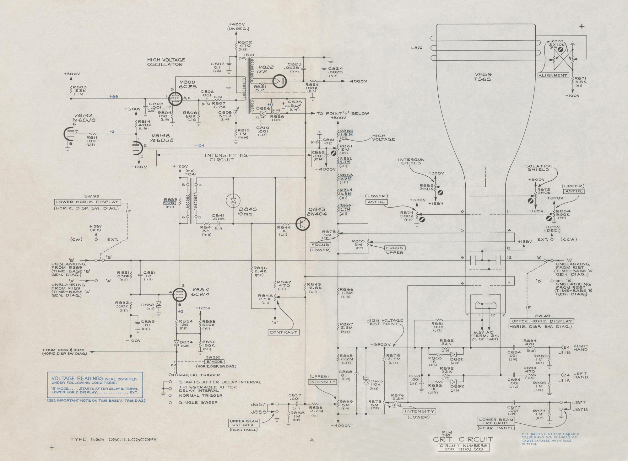
Refer to the Crt Circuit schematic in the back of this
manual. The oscillator is a modified Hartley which operates
at a frequency determined by the primary winding inductance and inter-turn capacitance of transformer T801. Oscillator frequency is not critical and is usually between 30 kc and 50 kc. The voltage on the screen grid of V800
determines the amplitude of the oscillator signal, which in turn determines the value of dc high voltage produced. This
property of the circuit is used to establish and maintain the
correct high voltage; -3900 volts.
The high voltage is applied to a high resistance voltage
divider which includes the INTENSITY, FOCUS, and HIGH VOLTAGE controls. With any particular setting of the HIGH VOLTAGE control, a certain percentage of the total voltage across the voltage divider is applied to the grid
of V814B. This grid voltage will always be about -103.5
volts, since it is the voltage actually being regulated. Since
the grid voltage is regulated and is a known fraction of the
high voltage, the high voltage will also be regulated.
When the voltage at the grid of V814B is -103.5 volts,
the voltage at the plate of V814B and the grid of V814A
will be about -2 volts. The voltage at the plate of V814A
and at the screen of V800 will be about +90 volts. If the
high voltage should change, the voltage at the grid of
V814B will also change. This change will be amplified by
V814B and V814A, thus changing the voltage on the screen
of V800. If, for example, the screen voltage is made more
positive, the oscillator signal amplitude will increase and
a greater dc high voltage will be produced.
Due to C862, the high gain of the error amplifier, and
the ability of the circuit to respond quickly, there is rarely
any significant variation in the high voltage. This is
because the correction for any change begins at nearly the
same instant as the change. Thus, a change is stopped
and corrected before it can become more significant.
Intensifying Circuit
The intensifying Circuit operates only when the TRIGGERABLE AFTER DELAY INTERVAL and STARTS AFTER DELAY INTERVAL modes of Time Base ‘B’ are used. Its only function is to dc couple a positive-going pulse to the upper beam CRT control grid. The normal voltage on this grid is about -3975 volts. The positive-going pulse at the control grid will cause a brightened segment within the upper beam trace.
(For more information about the purpose of
the brightened trace segment, see “Using the ‘B’ MODE Switch” in Section 2 of this manual.)
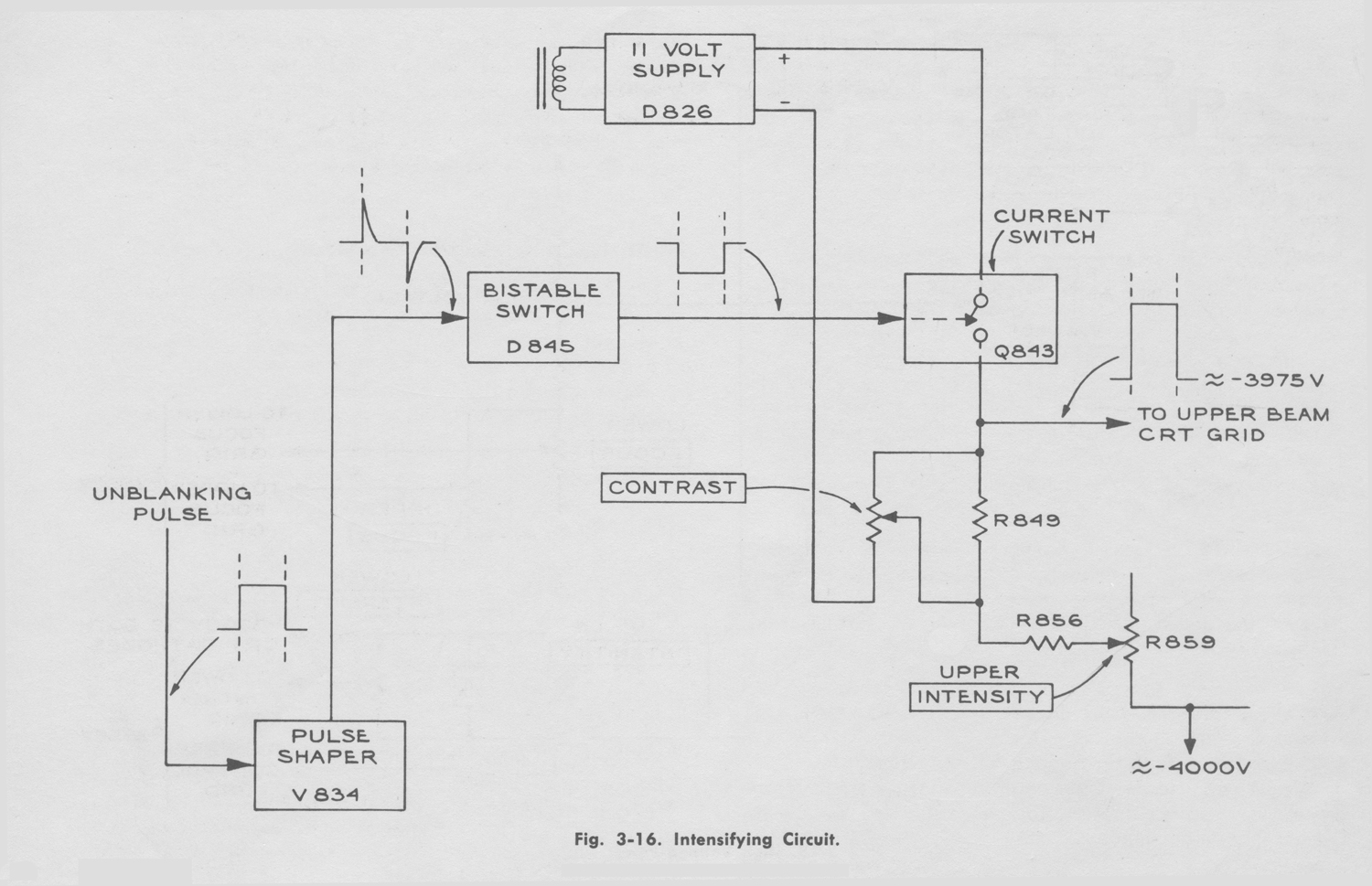
The basic elements of the intensifying Circuit are shown
in Fig. 3-16. Pulse Shaper V834 converts the applied
unblanking pulse into alternate positive and negative voltage pulses. These pulses actuate the bistable tunnel-diode switch D845 to produce a negative-going  turn-on pulse for Current Switch Q843.
When the Current Switch Q843 is open, the floating 11volt
supply does not produce a voltage drop across R849.
The voltage on the upper beam crt control grid during
this time depends entirely upon the setting of the INTENSITY control.  However, when the Current Switch is closed, current through R849 produces a voltage drop that drives the crt grid more positive. This causes a portion of the upper beam trace to be brightened.
For the following portion of the circuit description, refer
to the Crt Circuit schematic in the back of this manual.
The LOWER HORIZ. DISPLAY switch provides a choice
between three signal sources for unblanking  the crt: ‘A’
Unblanking, ‘B’ Unblanking, or +125 volts dc. Each of
these signals can cause the intensifying  Circuit to operate.
However, only the ‘B’ Unblanking signal will cause the
Intensifying  Circuit to produce an intensified crt display.
Hence, the following description assumes the use of the
‘B’ Unblanking signal.
If Time Base ‘B’ is not generating a sweep, the CRT
unblanking voltage from the LOWER HORIZ. DISPLAY switch is about  +25 volts and V834 is cutoff. When Time Base ‘B’ is then triggered, the unblanking voltage switches sharply to about +125 volts and V834 conducts heavily. (It is important  to note that the circuit operates only with the ‘B’ MODE switch in the STARTS AFTER DELAY INTERVAL or TRIGGERABLE AFTER DELAY INTERVAL position to provide cathode current for V834.) The sudden surge of current through T841 produces a sharp pulse in the secondary circuit.
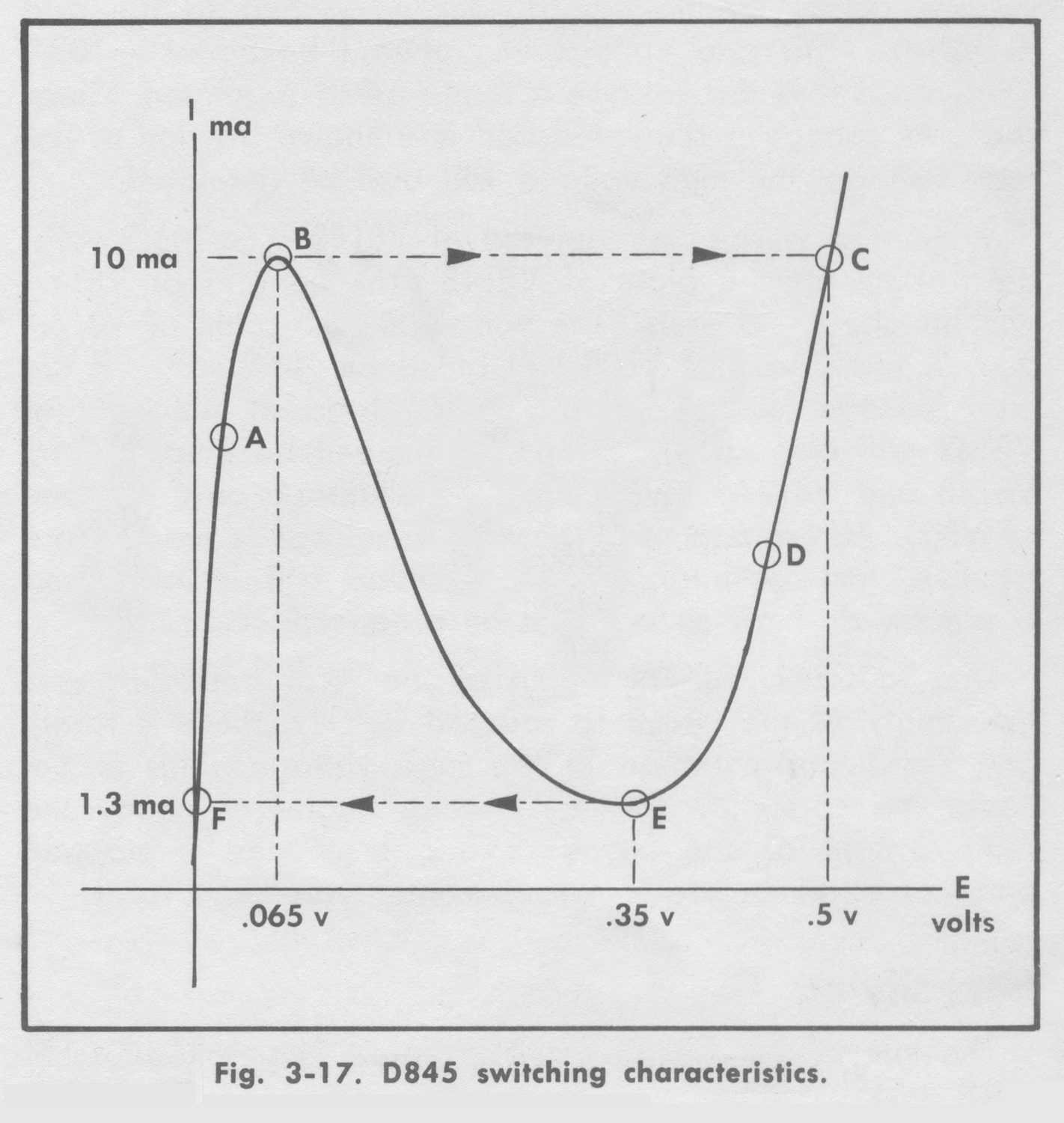
The dynamic characteristics of tunnel diode D845 are
shown in Fig. 3-17. Prior to the arrival of the pulse, the
tunnel diode maintains stable forward conduction at point
A on the curve. The voltage across the diode is then about
40 millivolts. This voltage is applied to the base-emitter
junction of Q843, but is not sufficient to cause the transistor
to conduct. Since there is no current through Q843, there
is no voltage drop across R849 and the voltage on the
upper beam crt control grid depends only on the setting
of the INTENSITY control (usually about -3975 volts at
normal trace brightness).
When the pulse is produced in the secondary circuit of
T841, the diode is driven through point B on the curve. The
diode is unstable at point B and therefore switches rapidly
to point C. As the input pulse subsides, the diode is unable
to continue operation at point C because R846 cannot satisfy the diode’s simultaneous demands for heavy current and high state voltage. Current then diminishes and the diode assumes stable operation at point D.
With the voltage across the diode now about 400
millivolts, Q843 is turned on. The current path is from the
positive end of C828, through Q843, R349, to the CONTRAST control (R848), and to the negative end of C828. The voltage drop thus produced across R849 drives the upper beam crt control grid several volts in the positive direction. This causes an increase in crt beam current and the trace becomes brighter.
When the unblanking  pulse ends, V834 is suddenly cutoff,
producing a pulse in the secondary circuit with polarity
opposite that of the previous pulse. The tunnel diode is
driven from operating point D (Fig. 3-17) through point E.
The diode is unstable at point E, and therefore switches
rapidly to point  F. At this point, R846 cannot satisfy the
diode’s demand for both low current and low state voltage.
Therefore, the current increases and the tunnel diode resumes stable operation at point A. The transistor reverts to cutoff, the upper beam crt control grid voltage drops to its
previous, more negative value, and the trace dims.
The CONTRAST control provides a means of controlling
the amplitude of the intensifying pulse and therefore the
amount of brightness increases during the brightened
segment of the upper beam trace. This is accomplished in the following manner.
As is true with most switches, transistor Q843 has a very
high series resistance when turned off and a very low series
resistance when turned on. Therefore, nearly all of the
11-volt supply voltage is dropped across R849 when Q843
is turned off. Hence, by controlling the total voltage
across the transistor and resistor, it is possible to control
the output pulse amplitude.
The CONTRAST control R848 and R847 form a voltage
divider across the 11-volt supply. By turning the CONTRAST control, the operator can vary the voltage across Q843 and R849 between about 2 and 11 volts.
Unblanking
A trace or spot can be obtained on the crt at all times
when an external signal is used for horizontal deflection.
However, such is not the case when horizontal deflection
is provided by one of the time base generators. When the
oscilloscope is used in the latter manner, a blanking signal
from the time base generator is applied to the crt. This
signal turns off the beam during sweep retrace and holds
it off until the next sweep begins.
Each of the two crt electron guns has a deflection plate
blanking system. A pair of deflection plates, similar to
those used for vertical and horizontal deflection, is placed
between the control and focus grids in each gun. One
plate in each pair is permanently connected to the +125
volt supply. The second plate can be connected to the
+125 volt supply or to one of the time base generators,
depending on the setting of the horizontal display switches.
The beam is constantly unblanked when the +125 volt
(EXT.) switch position is used.
If one of the time base generators provides horizontal
deflection for a particular beam, that beam will be
alternately blanked and unblanked in the following manner:
Between sweeps, the voltage applied to the crt blanking
plate by the time base generator will be about +25 to +30
volts With the other plate at +125 volts, the beam is
drawn into and absorbed by the more positive plate. Little
or no beam current gets past this point. When the time
base generator begins a sweep, it quickly increases the
voltage on the blanking plate to about +125 volts. Since
the blanking plate potentials are then essentially equal, the
beam current is released and passes on toward the face of
the crt to produce light.
Multi-trace Chopped Blanking
The Type 565 Oscilloscope can be used with multi-trace
plug-in units such as the Type 3A74. When this type of
plug-in unit is operated in the “chopped” mode, the
display may consist of up to four traces per beam. The plug-in forms the display by switching on each information-
channel, one at a time, in a rapidly repeating sequence.
The vertical signal information available at the output
of the plug-in during the very short time required to switch
channels, is of no value in the display. Hence, this information is blanked out.
A pulse from the plug-in unit is available at pin 24 of
the plug-in interconnecting jack when switching from one
channel to the next. This pulse is coupled through a dc
blocking capacitor to the appropriate crt cathode. The
pulse momentarily drives the cathode positive and cuts off
the beam current until the plug-in has finished switching
to the next channel.
Diodes D892 and D882 are dc restorers. They insure
equal trace brightness for the chopped and conventional
mode. They permit the crt cathodes to be driven positive
by the incoming signal, but prevent the cathodes from being
driven more negative than the voltage at the HIGH VOLTAGE TEST POINT; -3900 volts.
Intergun Shield and Isolation Shield
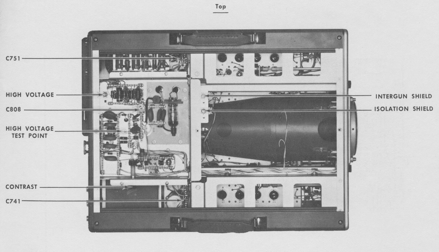
Proper adjustment of the INTERGUN SHIELD and ISOLATION SHIELD controls insures that (1) a straight line display will appear as a straight line, regardless of its position on the screen, and that (2) a display which is well focused at the center of the screen will also exhibit good focus at the edge of the screen. These controls also affect the deflection sensitivity and scan limits of the crt.
Trace Alignment
The trace alignment coil surrounds the crt at a point
about 6 inches behind the face plate. The plane of the
coil is parallel to the plane of the face plate. The TRACE
ALIGNMENT control determines the amount and direction
of the dc current through the coil. By adjusting this control,
the entire display can be rotated a few degrees clockwise
or counterclockwise about the axis of the crt.
Display alignment is affected by the earth’s magnetic
field and may change when the instrument is moved. In
such cases, the operator can quickly realign the display
with the graticule markings by adjusting the TRACE
ALIGNMENT control.
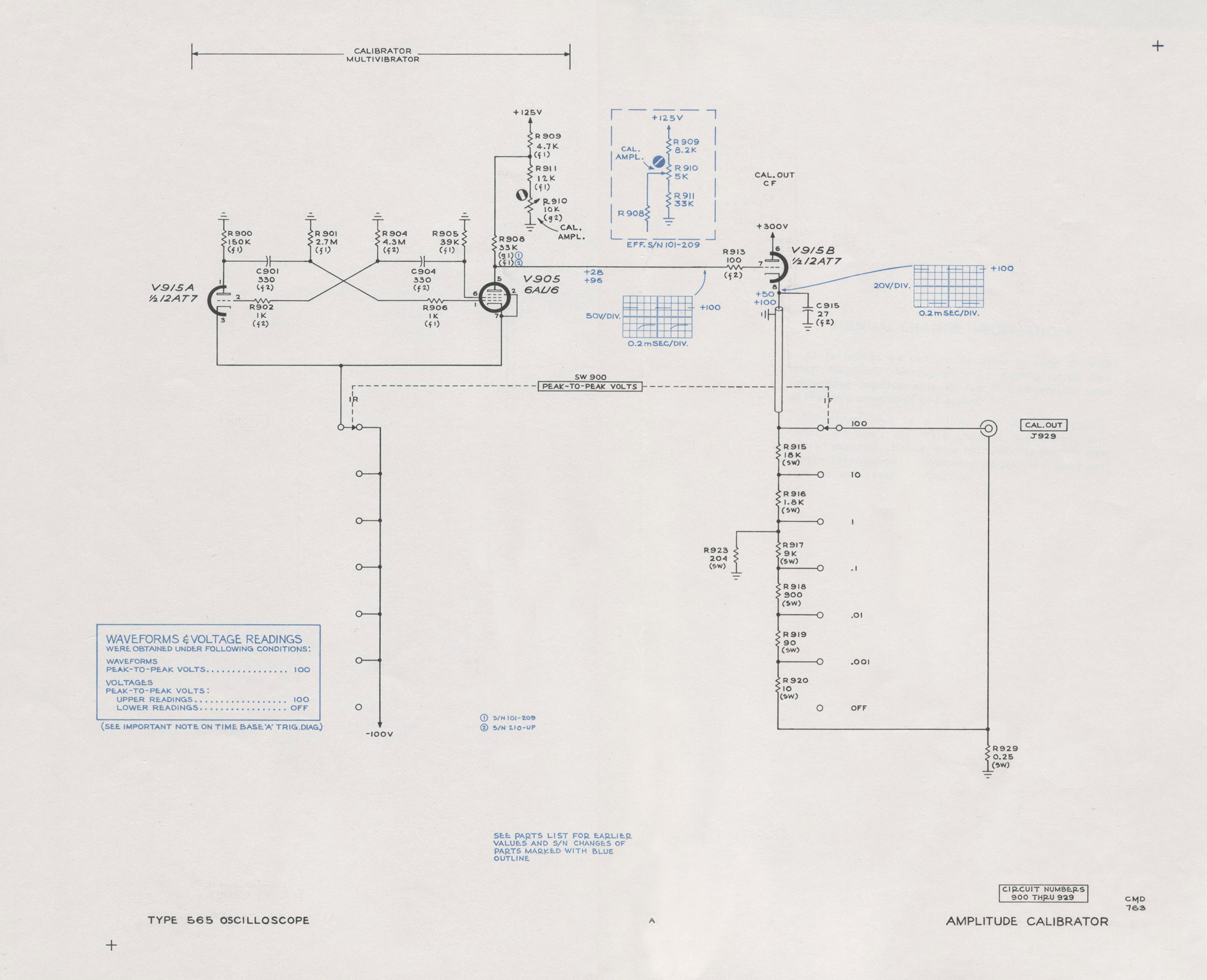
AMPLITUDE CALIBRATOR
The Amplitude Calibrator generates square waves of an
accurate peak-to-peak voltage available in six steps at the
CAL. OUT connector. The square wave output is positive-
going from ground. The frequency is about one kc, rise and
fall times are several microseconds, and the duty factor is
about  0.5. Because of its intended use, only the peak-to-
peak voltage accuracy of the Amplitude Calibrator is given
a specific tolerance.
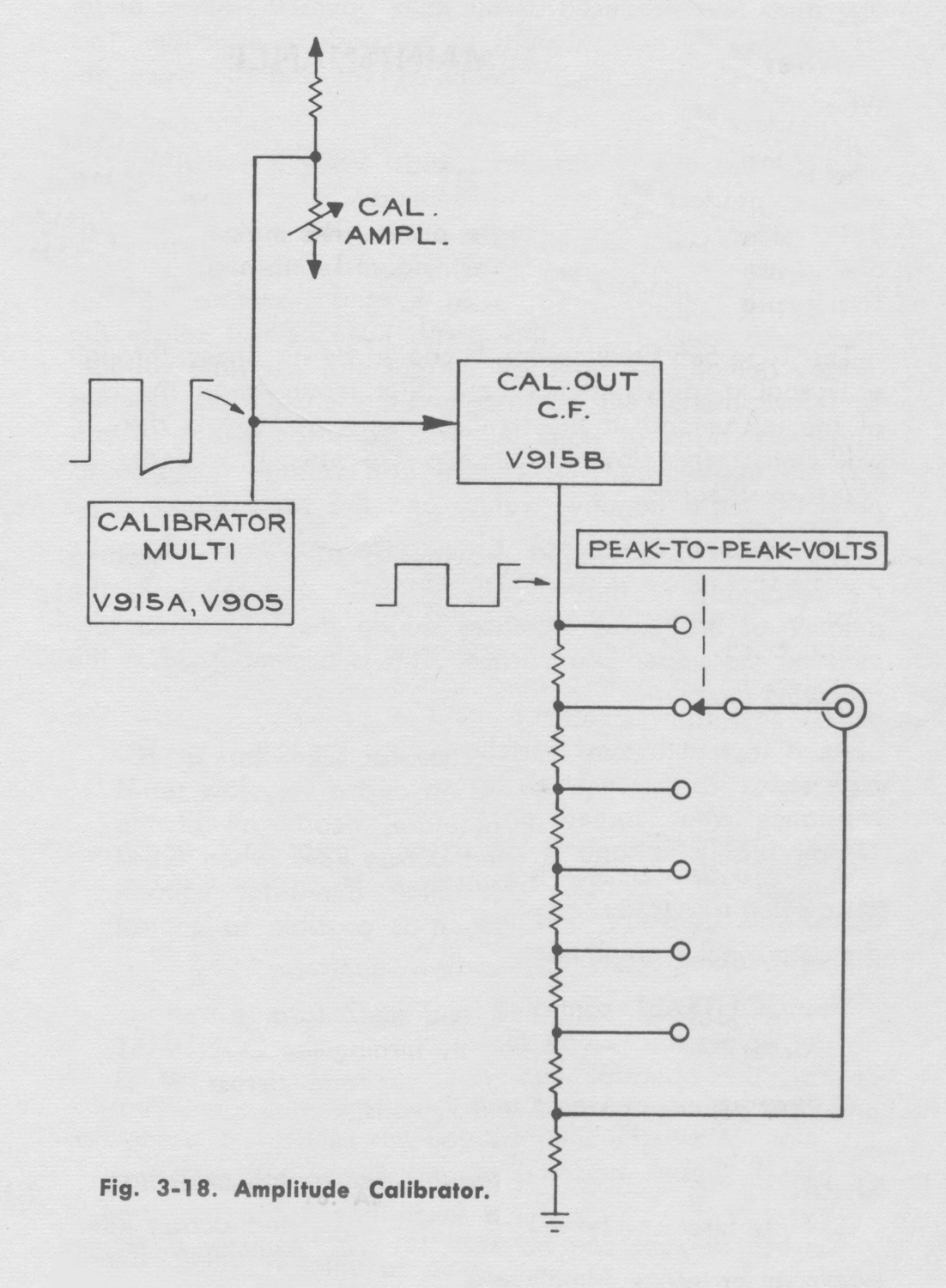
Refer to the block diagram, Fig. 3-18. The Amplitude
Calibrator consists of an astable multivibrator, an output
cathode follower, and a precision output divider. The
multivibrator switches the cathode follower alternately between cutoff and conduction. The cathode follower output voltagis an accurate +100 volts during conduction and zero volts during cutoff. The output divider provides five lower amplitudes from the basic 100 volt square wave. The CAL. OUT voltage is selected by setting the PEAK-TO-PEAK VOLTS switch to the desired value.
Refer to the Amplitude Calibrator schematic diagram in
the back of the manual.
V915A and V905 form a conventional astable plate
coupled multivibrator.  In the multivibrator action, V905
operates as a triode with the screen grid acting as the
plate. When V905 conducts, a portion of the cathode
current goes to the pentode plate and drops the plate voltage
to about  -20 volts. This voltage is applied to the grid of
V915B. V915B is cutoff and its cathode voltage is zero.
When V905 is cut off, the voltage at its plate is
determined by the voltage divider; R909, R910, and R911. The CAL. AMPL. control, R910, is set during calibration so the voltage at the cathode of V915B will be exactly +100
volts when V905 is cut off.
A 0.25 ohm resistor located between the CAL. OUT coax
connector and ground is approximately equal to the
resistance of the braid of a 42 inch long RG-58A/U coax
cable. Its purpose is to cancel any coax braid ground
current effects on calibrator voltage accuracy that may exist
when the Type 565 AMPLITUDE CALIBRATOR is used as a signal source between the oscilloscope and some other
instrument chassis. The ground currents in this case are
usually developed in the ac power line third-wire grounding
system when the Type 565 and the other instrument
chasses are supplied from different convenience outlets».
§§§
Abbiamo omesso la pur interessante sezione MAINTENANCE del manuale delle istruzioni.
Per consultare le altre schede dedicate a questo oscilloscopio esposto al museo MITI (su proposta di Fabio Panfili) scrivere “565” su Cerca.
Elaborazioni di Fabio Panfili.
Per ingrandire le immagini cliccare su di esse col tasto destro del mouse e scegliere tra le opzioni.
 

Oscilloscope Tektronix Type 565 serial 689, seventh part (MITI Museum)

Oscilloscopio Tektronix Type 565. Settima parte.
Nell’inventario D del 1956 si trova al n° 3747 e risulta acquistato nell’agosto del 1964; vi si legge: “Silvestar ltd. Milano. Oscilloscopio Tektronix mod. 565 matr. 689. Dest. Elettronica ₤ 1·678·600”. Insieme alla fotocamera che è al n° 3746, dove si legge: “Silvestar ltd. Milano. Macchina fotografica Tektronix mod. C-12 completa di Bezel-Tektronix. Dest. Elettronica. ₤ 557·700”.
Il testo continua dalla sesta parte.
§§§
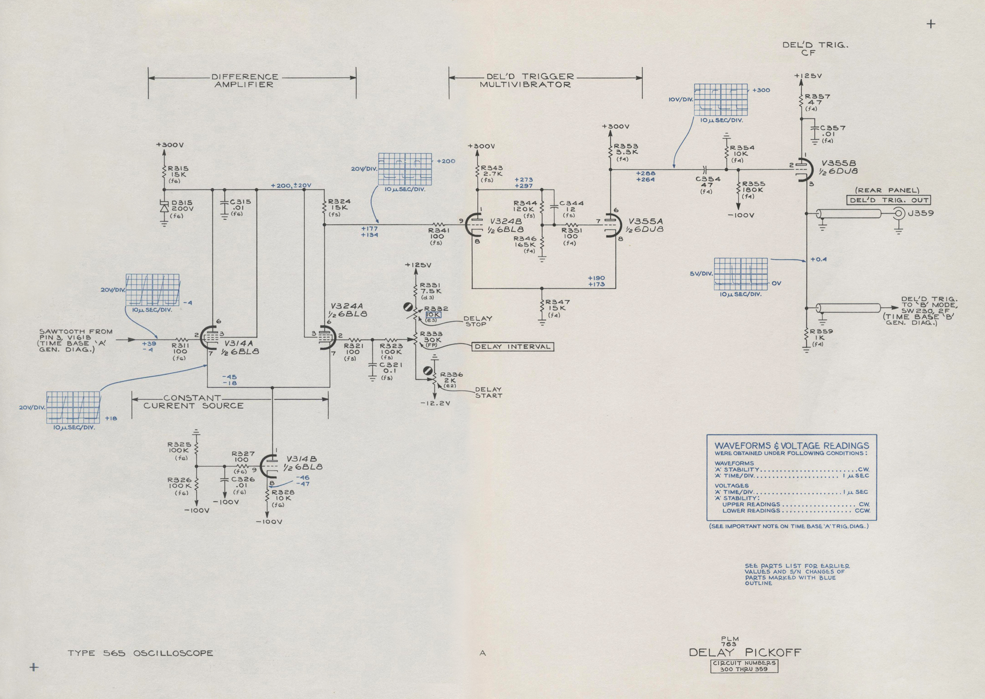
                  «DELAY PICKOFF

The Delay Pickoff circuit generates a positive-going,
differentiated pulse at a predetermined time during each
sawtooth  produced by Time Base ‘A’. The pulse is available at the rear panel for external use and is also coupled to the ‘B’ MODE switch. The relationship between this pulse and Time Base ‘B’ is discussed later in this section under “Time Base ‘B’ Lockout”.

Block diagram, Fig. 3-8, shows the four basic sub-circuits in the Delay Pickoff. The sawtooth output of Time Base ‘A’
is applied to the Difference Amplifier. The Difference Amplifier compares the sawtooth voltage to a variable dc
voltage from the DELAY INTERVAL control. If the voltage
from the DELAY INTERVAL control is more positive than the instantaneous sawtooth voltage, the Difference Amplifier output will be a low positive voltage. If the sawtooth voltage is the more positive, the output will be a somewhat higher positive voltage. It is important to note that the transition from the lower to the higher output voltage is actually  an amplified segment of the input sawtooth as shown on the block diagram.
The Delayed Trigger Multivibrator converts the Difference
Amplifier output signal into a fast-rise pulse. This pulse is
then differentiated and clipped so only the positive-going
pulses appear at the output of the Delayed Trigger Cathode
Follower.
The point along the sawtooth rise where the delayed trigger
output pulse will occur is determined by the voltage from the DELAY INTERVAL control. If a low voltage is selected, the pulse will occur during the early portion of the
rise while the sawtooth voltage is low. If a higher voltage is selected, the pulse will occur at some later time during the rise when the sawtooth voltage is proportionally higher.
The maximum delay that can be obtained is slightly less
than the total time duration of the sawtooth rise, which is
determined by the setting of the ‘A’ TIME/DIV. switch. For
example, if the ‘A’ TIME/DIV. switch is set to 1 mSEC, the
maximum DELAY INTERVAL dial setting of 10.00 would result in a 10 millisecond delay between the start of the ‘A’
sawtooth and the delayed trigger pulse output.
The following detailed description refers to the Delay
Pickoff schematic in the back of this manual.
Constant Current Tube
V314B is a constant current source for the Difference Amplifier. The voltage divider formed by R325 and R326
applies about  -50 volts to the grid. This stable grid voltage and the high resistance in the cathode circuit force a constant 5 ma to flow through the tube. The Difference
Amplifier will conduct this fixed current, either through one tube or shared between the two tubes.
Difference Amplifier
In the Difference Amplifier, the cathodes of V314A and
V324A are connected together. The tube having the more
positive control grid voltage will determine the voltage on the cathodes of both tubes. For example, assume that the
DELAY INTERVAL control is set to 4.00. The voltage at
the grid of V324A will then be about +36 volts. If Time
Base ‘A’ is in the quiescent state, the voltage at the grid
of V314A will about -3.5 volts. Since the grid of V324A
is more positive, it will establish the common cathode voltage at about +38 volts. Therefore, V314A is deep into cutoff.
V324A conducts and the voltage at its plate is about +121 volts.
As V324A cuts off, its plate voltage rises from about +120
age at the grid of V314A rises. Since V314A is deep in cutoff, the rising voltage does not immediately affect the
Difference Amplifier. But as the sawtooth voltage rises
through the range from about 2.5 volts below to 2.5 volts
above the voltage from the DELAY INTERVAL control, V314A comes out of cutoff and into full conduction. The conduction of V314A forces V324 to reduce conduction. Then, as the sawtooth voltage becomes more positive than the DELAY INTERVAL control voltage, the common cathode voltage rises and cuts off conduction in V324A.
As V324A cuts off, its plate voltage rises from about +120
volts to about +200 volts. The elapsed time from the beginning to the end of this voltage change depends upon the Time Base ‘A’ sweep rate; about 2 seconds at 5 seconds per division and about 0.5 microsecond at 1 microsecond per division. The Delayed Trigger Multivibrator (a Schmitt trigger) converts this variable rate of rise into a voltage step of consistently fast risetime which is independent of the Time Base ‘A’ sweep rate.
Delayed Trigger Multivibrator
When the voltage at the plate of V324A is at the lower
level (about +120 volts), V324B in the Delayed Trigger
Multivibrator is cut off and V355A is conducting.  As the
voltage at the plate of V324A rises to about +170 volts
and V324B begins to conduct, the voltage at the plate of V324B drops slightly, lowering the voltage at the grid of
V355A. This reduces the current through V355A. However,
the voltage at the grid of V324B will not permit the
common cathode voltage to drop. Hence, the current given up by V355A is immediately assumed by V324B. This reduces the voltage at the plate of V324B still more, compounding the initial action. Thus, the beginning of conduction in V324B causes the Delayed Trigger Multivibrator to rapidly change states; V324B conducts and V355A cuts off. This produces a fast-rise positive-going voltage step at the plate of V355A.
Delayed Trigger C.F.
The voltage step produced by the Delayed Trigger
Multivibrator is differentiated by the network consisting of C354, R354, and R355, and is applied to the grid of V355B.
Delayed Trigger Cathode Follower V3558 is held near cutoff by R354 and R355. When the delayed trigger pulse appears at the grid, the tube conducts heavily and the pulse isreproduced across R359.
The entire Delay Pickoff circuit resets during the retrace time of the Time Base ‘A’ sawtooth when the voltage at the
plate of V324 drops below about +155 volts. When the
differentiated pulse at the grid of V355B subsided, the tube was again near cutoff. Hence, when the negative going
reset pulse at the grid of V355B drives the tube deeper into
cutoff, very little negative going output signal is produced.
Several important conditions exist at the instant the
delayed trigger output pulse occurs:
1. The voltage from the DELAY INTERVAL control essentially equals the instantaneous sawtooth voltage.
2. Time Base ‘A’ trace will have moved as many graticule
divisions as the DELAY INTERVAL dial setting (10X MAG. off).
3. The time delay between the start of the ‘A’ sawtooth and
the delayed trigger output pulse will equal the DELAY
INTERVAL dial indication times the ‘A’ TIME/DIV. switch
setting.
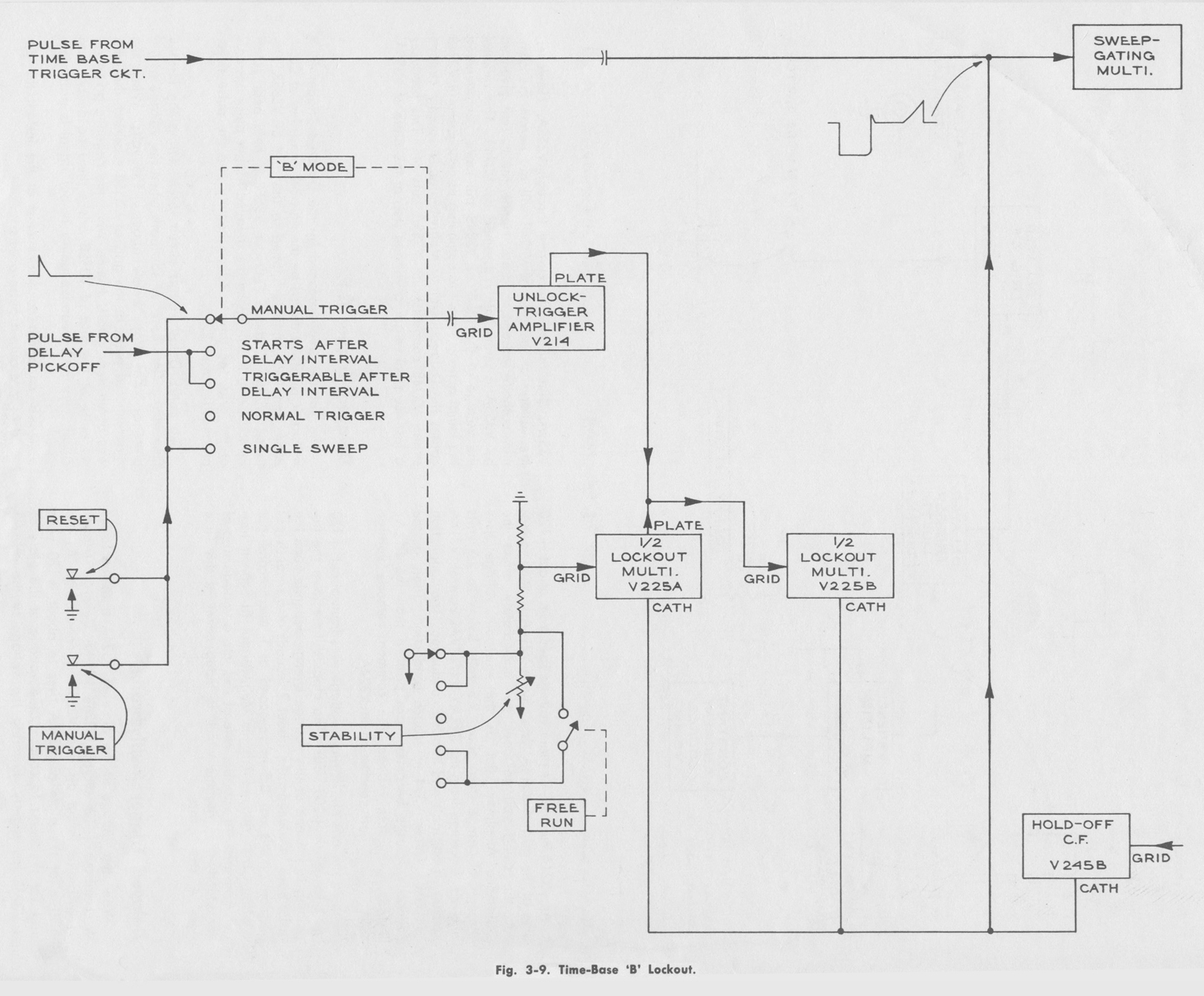
            TIME BASE ‘B’ LOCKOUT
As previously mentioned in the description of Time Base
‘A’, the STABILITY control and FREE RUN switch settings determine whether the time base will be inoperative, triggerable, or will free run. Time Base ‘B’ operates in exactly the same manner when the ‘B’ MODE switch is set to NORMAL TRIGGER. However, when the ‘B’ MODE switch is in any other position, there is one additional factor controling Time Base ‘B’; the Lockout Multivibrator.
The Lockout Multivibrator is a bistable electronic switch.
In one state, it permits the STABILITY control or associated switches to have full control of the time base, just as they do in Time Base ‘A’. In the other state, the Lockout Multivibrator over-rides the function of these controls and renders the time base inoperative.
At the beginning of a Time Base ‘B’ sequence, the Lockout
Multivibrator holds the time base in the “Time Base
inoperative” state. A pulse from the Unlock-Trigger
Amplifier will switch the multivibrator to the “Time Base
Operative” state and Time Base ‘B’ then either free runs or
becomes triggerable. When Time Base ‘B’ completes one
sawtooth, the Lockout Multivibrator resets to the “Time Base Inoperative” state. This sequence repeats for each sawtooth produced by Time Base ‘B’.
The following information is closely related to the
STABILITY control discussion under “Time Base Generators” in an earlier portion of this section. For better understanding of Time Base ‘B’ Lockout, the STABILITY control discussion should be read first.
Unless otherwise stated in the following descriptions, the
‘B’ STABILITY control is set for triggered operation and
the ‘B’ MODE switch places the Lockout Multivibrator  into one of the following modes of operation.

Single Sweep Mode
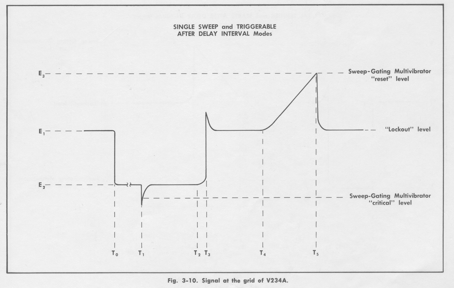
Refer to the block diagrams, Fig. 3-9 and Fig. 3-10 during
the following descriptions. Fig. 3-10 represents the signal
at the grid of V235A during one cycle of operation as follows:
1. Before to, V225B conducts during the “Lockout” period and holds the grid of V235A at voltage level E1. At this voltage level, the Sweep-Gating Multivibrator cannot be triggered, nor will it free run.
2. When the Single Sweep RESET button is pushed (t0), V225B cuts off. The grid voltage of V235A drops sharply to the level where V225A conducts.
3. The STABILITY control determines the voltage (E2) that
V225A applies to the grid of V235A. The time base is now
in the normal quiescent state and only requires a pulse from
the Time Base Trigger circuit to start the sawtooth. This
could occur immediately or at some indefinite later time.
4. When a trigger pulse is received (t1), the sawtooth cycle
will begin.
5. As the sawtooth reaches about one-half its final
amplitude, the Hold-Off Cathode Follower, V245B, begins to conduct (t2) and V225A cuts off (t3).
6. As V225A cuts off, V225B again comes into conduction
(t3) and raises the grid voltage of V235A to the “Lockout”
level (E1). This voltage level is well below the “reset” level
of the Sweep-Gating Multivibrator and therefore has no
effect on the output sawtooth now in progress.
7. When the output sawtooth reaches about three-fourths its
final amplitude, V245B begins to conduct again (t4) and
V225B cuts off. The sawtooth feedback raises the grid voltage of V235A to the reset level (E3) and stops the sawtooth (t5) in the normal manner.
8. As V2458 continues to conduct, it reproduces part of the
sawtooth retrace at the grid of V235A. But as the voltage
approaches the “Lockout” level (E1) V225B again conducts
and V245B cuts off.
9. The voltage at the grid of V235A is now stable at the
“Lockout” level (E.). The cycle is complete and cannot
repeat until the Single Sweep RESET button is pushed again.
Triggerable After Delay Interval Mode
This mode differs from the Single Sweep mode in that
the “unlocking” pulse comes from the Delay Pickoff Circuit
instead of the RESET push button. Also, the Time Base
‘B’ LEVEL control FREE RUN function is disconnected.

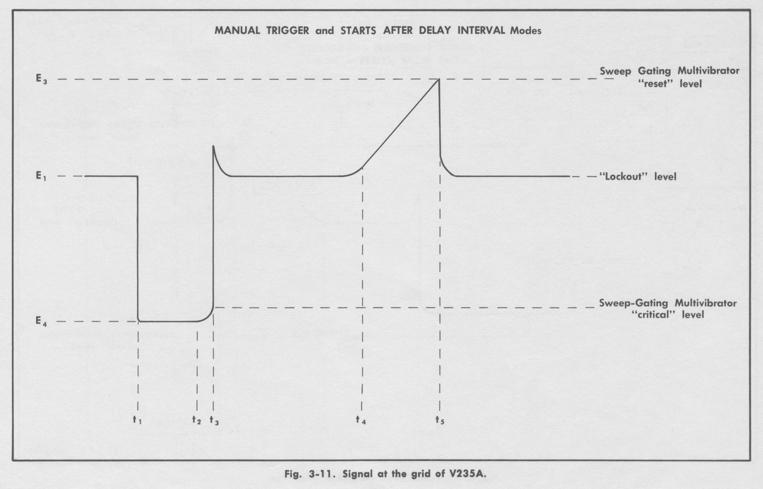
Manual Trigger Mode
The differences between this mode and the Single Sweep
mode are as follows:
1. The “unlocking” pulse comes from the MANUAL TRIGGER push button instead of the RESET push button.
2. When the voltage drops at to (see Fig. 3-11), it drops to
a more negative level (E4) than in the Single Sweep mode.
This level is below the “trip” level of the Sweep-Gating
Multivibrator. Hence, the sawtooth cycle begins
immediately without waiting for a pulse from the Time Base Trigger circuit. This occurs because the ‘B’ MODE switch by-passes the STABILITY control and causes V225A to conduct at the lower level.
Starts After Delay Interval Mode
The only difference between this mode and the Manual
Trigger mode is that the “unlocking” pulse comes from the
Delay Pickoff Circuit instead of the MANUAL TRIGGER push button.
Refer to the Time Base ‘B’ schematic in the back of this
manual during the following description. For the remainder
of this description, the ‘B’ MODE switch can be assumed to
be set at any position except NORMAL TRIGGER.
Since there are two negative feedback paths between
V225A and V225B (pin 6 to pin 9 and pin 8 to pin 7), the
two tubes cannot conduct at the same time. When the time
base is “locked out”, V225B conducts and holds the cathodes of V225A and V245B considerably more positive than their grids. Hence, these two tubes are cut off.
The Unlock-Trigger Amplifier, V214, is self- biased near
cutoff. The positive-going  “unlocking” pulse applied to the
control drives V214 into heavy conduction and produces
a high amplitude negative-going pulse at the plate. This
pulse is applied to the grid of V225B through C223-R223,
driving its cathode considerably more negative than the grid
of V225A, causing V225A to suddenly conduct. The voltage at the plate of V225A is already low in the presence of the negative-going pulse from the Unlock—Trigger Amplifier.
Therefore, V225A conducts as a triode with its screen grid
acting as the triode plate. As the pulse at the plate subsides
and the plate voltage tends to rise, a greater portion of the
cathode current in V225A flows to the pentode plate. Thus,
the voltages at the pentode plate of V225A and at the grid
of V225B do not rise after the pulse has subsided. V225A
remains in conduction and V2258 is cut off.
With V225B now conducting, the common cathode voltage
is determined by the switches and STABILITY control in the tube’s control grid circuit. This is exactly the same condition that exists when the time base is operated in the NORMAL TRIGGER mode. The time base will either free run or awaita trigger pulse, depending upon the switch settings in the grid circuit of V225A.
From this point, the cycle continues to the end of the
sawtooth rise as previously described.
At the end of the sawtooth rise, V245B has raised the
common cathode voltage so that both V225A and B are
cut off. When both tubes are cut off, V225B has the more
positive control grid voltage. Hence, as the common cathode voltage goes more negative during the retrace portion of the sawtooth, V225B will come into conduction while V225A is still deep in cutoff. With the cycle completed and V225B conducting, the time base is again “locked out”. The LOCKOUT LEVEL control is adjusted during calibration to set the conduction level of V225B. Whenever V225B conducts, the common cathode voltage should be about half way between the reset and trip voltages of the Sweep-Gating Multivibrator.
The READY lamp lights only when V225B is cut off. The
lamp therefore shows the operator whether or not the Sweep
Gating Multivibrator is ready to operate.
             HORIZONTAL AMPLIFIER
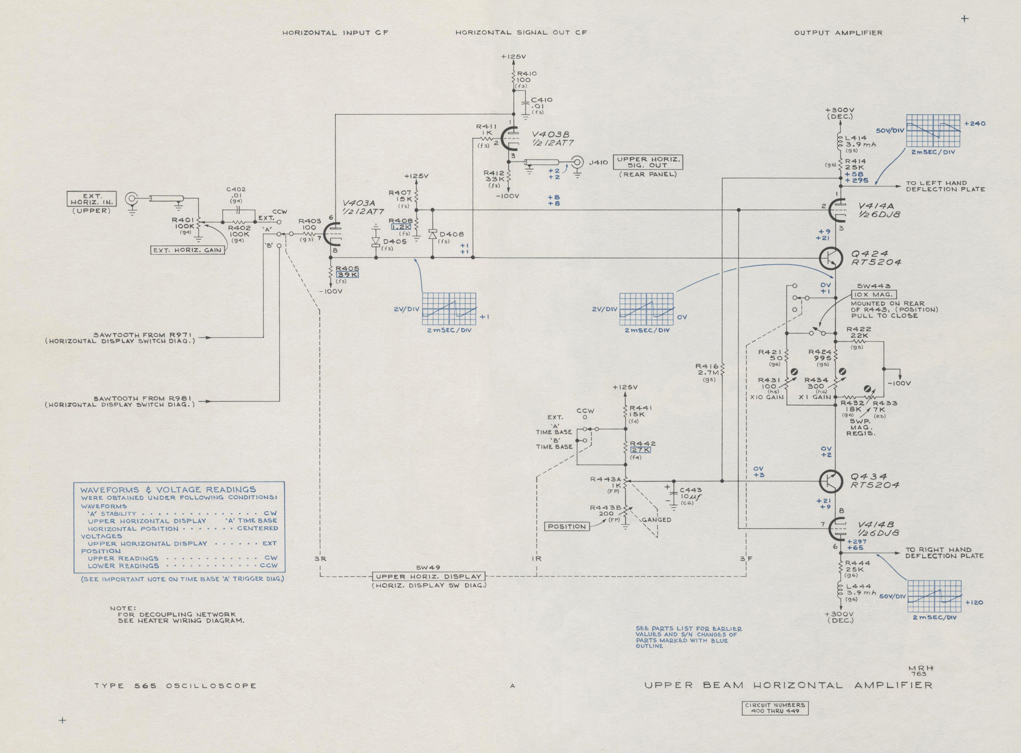
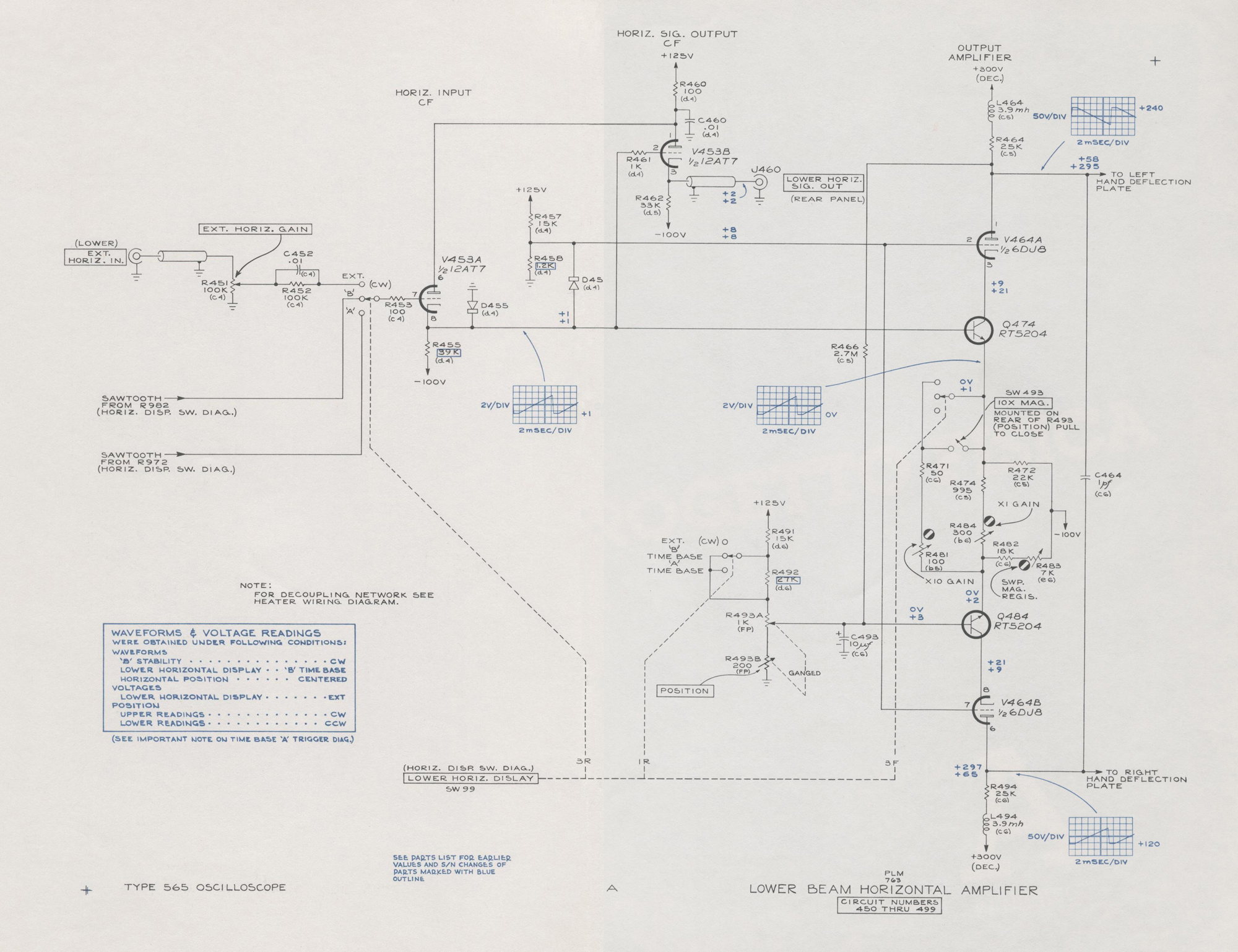
The Upper and Lower Beam Horizontal Amplifiers are
nearly identical. The following descriptions apply to both
amplifiers, but the Upper Beam Horizontal Amplifier circuit
reference numbers are used.
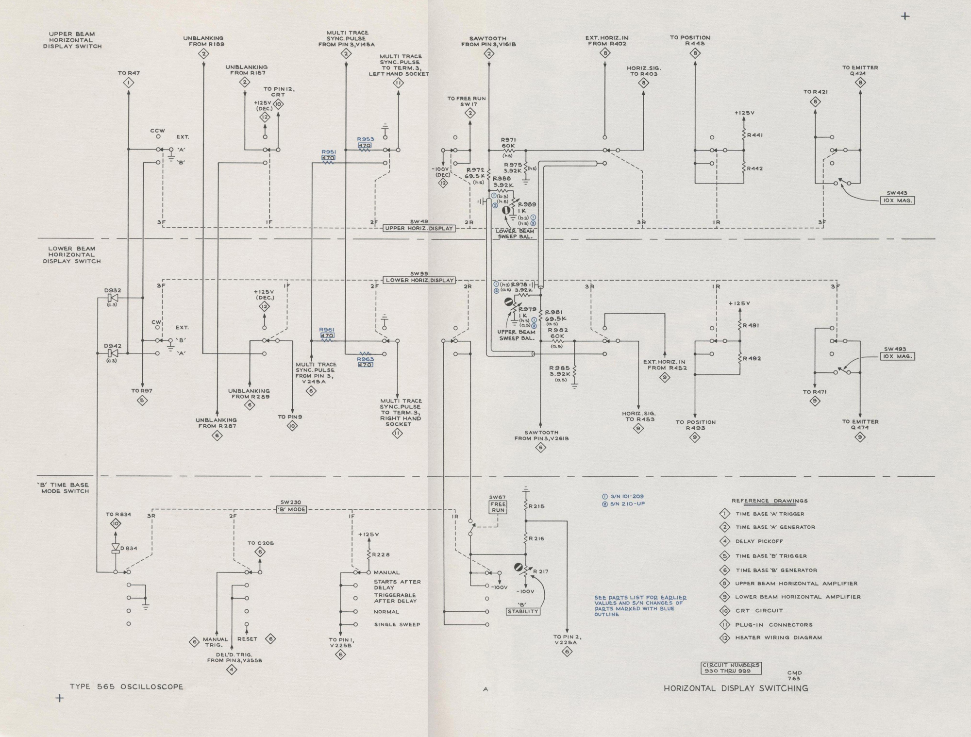
The Horizontal Amplifier input signals can come from Time
Base ‘A’, Time Base ‘B’, or from an external source. The
appropriate signal is selected by setting the Horizontal Display switch.
Each Horizontal Amplifier has two outputs; a push-pull
output connected to one pair of CRT horizontal deflection
plates and a single-ended output at the rear panel for external use. The operator can increase the gain of the push-pull portion of the amplifier ten times by turning on the ten times magnifier (10X MAG.).

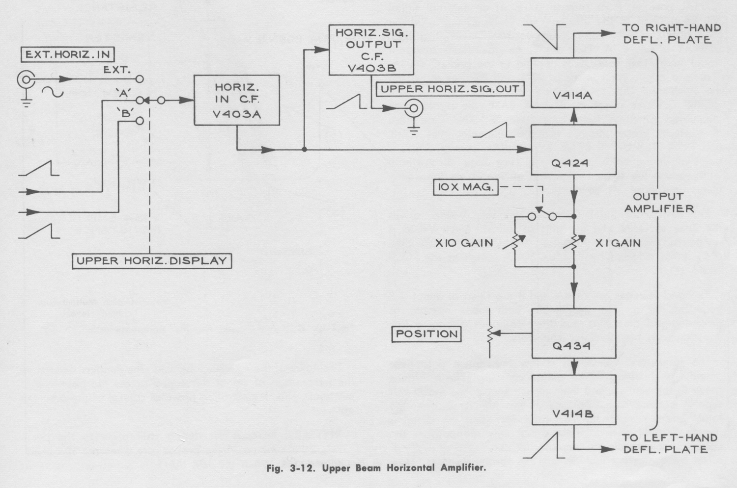
The block diagram, Fig. 3-12, shows the basic sub-circuits
in the Horizontal Amplifier. V403A isolates the amplifier
from the signal source and provides a law driving impedance for Q424. V403B isolates the amplifier from any reasonable load impedance connected to the rear panel horizontal signal output connector.
Q424, V414A, Q434, and V414B form a paraphase
amplifier. The signal applied to Q424 varies the current
through both Q424 and Q434. The current variations pass
through V414A and B and produce a high amplitude voltage swing at the amplifier output. When the 10X MAG. switch is closed (pulled out) the resistance between the emitters of the transistors is decreased and the gain is increased ten times. The POSITION control determines the dc average voltage difference between the right and left hand deflection plates.
Refer to the Upper Beam Horizontal Amplifier schematic
in the back of the manual during the following description.
When the UPPER HORIZ. DISPLAY switch is in the
EXTERNAL position, from zero to 100% of an external signal will be applied to the grid of V403A, depending upon the EXT. HORIZ. GAIN control setting. When UPPER HORIZ. DISPLAY is set to ‘A’ TIME BASE, an attenuated sawtooth signal from Time Bose ‘A’ is applied to the grid of V403A.
The fixed attenuator consists of R971 and R975 as shown on the Horizontal Display Switching schematic. When UPPER HORIZ. DISPLAY is set to ‘B’ TIME BASE, the signal is an attenuated sawtooth from Time Base ‘B’. The Time Base ‘B’ sawtooth passes through variable attenuator R981, R978, and R979. The UPPER BEAM SWEEP BAL. control, R979, is adjusted during calibration so the Time Base ‘B’ sawtooth will produce the same sweep rate on the crt as the equivalent Time Base ‘A’ sawtooth.
The Horizontal Input Cathode Follower, V403A, drives
the base of Q424 and the grid of V403B. Since V403B is
ahead of the Output Amplifier, the UPPER HORIZ. SIG.
OUT is not affected by the 10X MAG. switch or the
POSITION control.
The grid voltages on V414A and B are fixed at about  +8
volts by the divider, R407-R408. Both tubes operate as
grounded-grid amplifiers and their cathodes present a low
impedance to the transistor collectors.
The transistors operate as a low impedance paraphase
amplifier with degenerative emitter coupling. The resistance
between the emitters and their current source, the -100 volt
supply, is quite high. Because of this high resistance, the
total current through the two transistors (and the tubes) is
nearly constant and an input signal only reapportions the
current. For example, an increase in current through Q424 is offset by a nearly equal decrease in current through Q434.

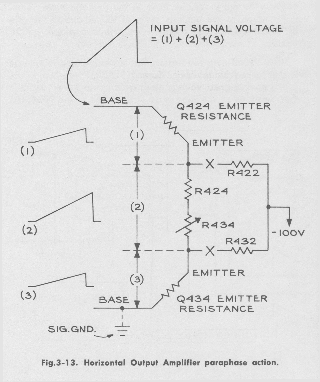
Fig. 3-13 shows how the input signal increases current
through one transistor while equally decreasing current
through the other. The input signal is distributed across the series resistances beginning at the internal emitter resistance of Q424 and ending with the internal emitter resistance of Q434. Since the external circuit is balanced for the two transistors, their internal emitter resistances are equal. Hence, the signal voltages developed across the base- emitter junctions will be equal.
Fig. 3-13 shows that the base of Q424 goes positive with
respect to its emitter while the emitter of Q434 goes
positive with respect to its base. Thus, the two transistors see equal, but opposite phase, input signals. The current
increases through Q424 and decreases through Q434. These
current variations pass through the tubes and develop the
output signal across the plate load resistors.
The value of the resistance between the emitters determines
the percentage of signal developed across the base-emitter
junctions. This degeneration provides control of the amplifier gain.
X1 GAIN, R434, is set during calibration so the beam
moves across the crt at the proper rate when the 10X MAG.
is turned off. When the 10X MAG. is turned on, the series
combination of R421 and R431 is in parallel with R424 and
the X1 GAIN control. The emitter coupling resistance is
decreased and the amplifier gain is increased. X10 GAIN is
set during calibration so the amplifier gain is exactly ten
times greater with the 10X MAG. turned on than with it off.
The current source resistors, R422 and R432, are shown
disconnected in Fig. 3-13 to illustrate that the signal changes the total current through them very little. However, due to the signal across the emitter coupling resistance, the current through R432 decreases slightly while it increases slightly through R422.
When the transistor base voltages are equal, the transistor
currents should also be equal so the beam will be at the
horizontal center of the crt. When the 10X MAG. is turned
on, the emitter coupling resistance is small and the current
will essentially balance. But, when the 10X MAG. is turned
off, the greater resistance can cause a current imbalance, if
the two halves of the amplifier are not exactly equal. Hence,
the SWP. MAG. REGIS., R433, is adjusted during calibration to balance the current with the 10X MAG. turned off. Then, when the beam is at the center of the crt with the 10X MAG. an, it will remain at the center when the 10X MAG. is turned off ».
§§§
Il testo prosegue nella ottava parte.
Per consultare le altre  schede dedicate a questo oscilloscopio esposto al museo MITI (su proposta di Fabio Panfili) scrivere “565” su Cerca.
Elaborazioni e testo a cura di Fabio Panfili.
Per ingrandire le immagini cliccare su di esse col tasto destro del mouse e scegliere tra le opzioni.


Oscilloscope Tektronix Type 565 serial 689, sixth part (MITI Museum)

Oscilloscopio Tektronix Type 565. Sesta parte.
Nell’inventario D del 1956 si trova al n° 3747 e risulta acquistato nell’agosto del 1964; vi si legge: “Silvestar ltd. Milano. Oscilloscopio Tektronix mod. 565 matr 689. Dest. Elettronica ₤ 1·678·600”. Insieme alla fotocamera che è al n° 3746, dove si legge: “Silvestar ltd. Milano. Macchina fotografica Tektronix mod. C-12 completa di Bezel-Tektronix. Dest. Elettronica. ₤ 557·700”.
Il testo continua dalla quinta parte.
§§§

                                  «SECTION 3
                     CIRCUIT DESCRIPTION
General
This portion of the Instruction Manual presents a detailed
discussion of the Type 565 circuitry operation. This discussion refers to various block diagrams inserted in the text, and to the circuit diagrams in the back of this manual.
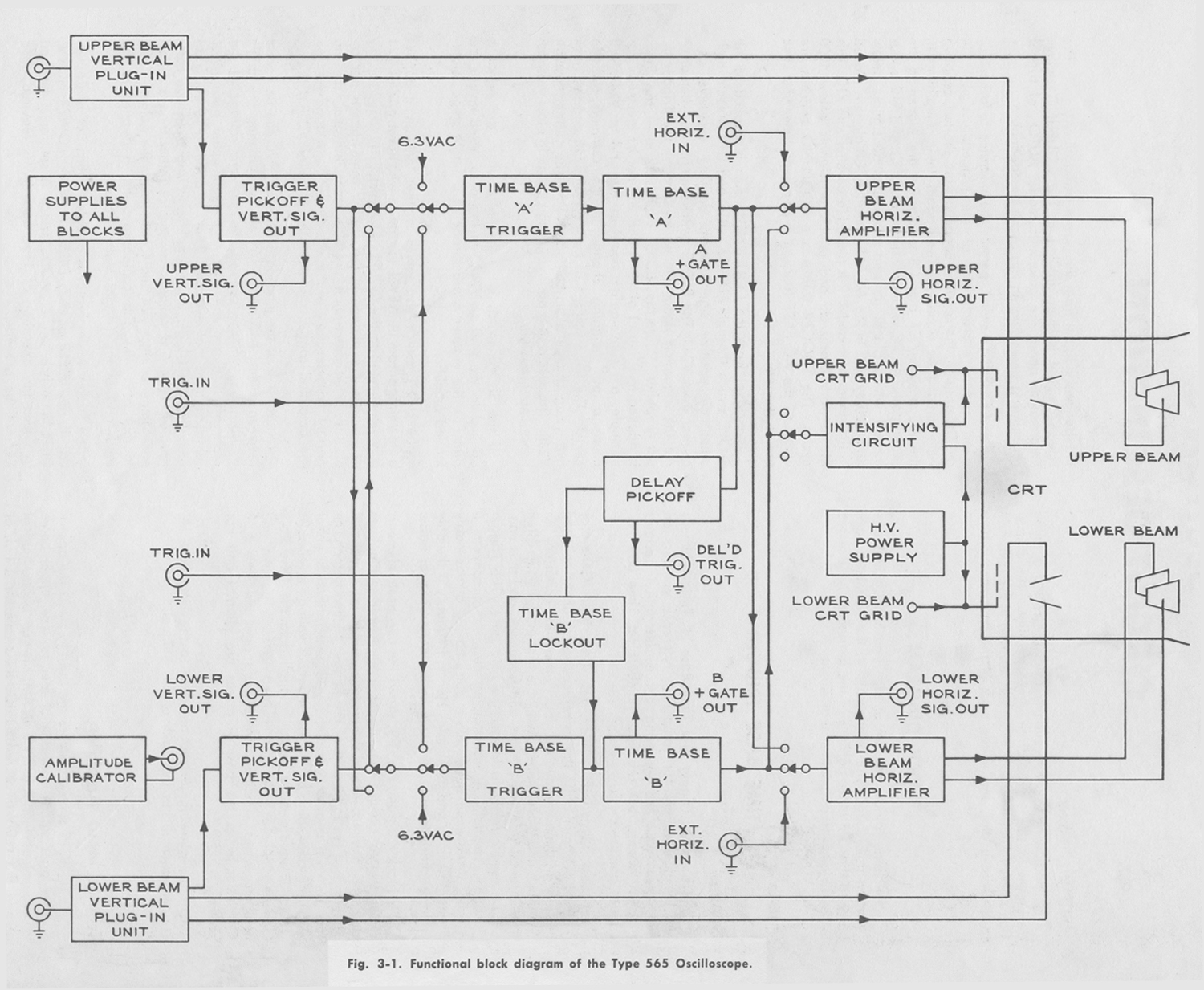
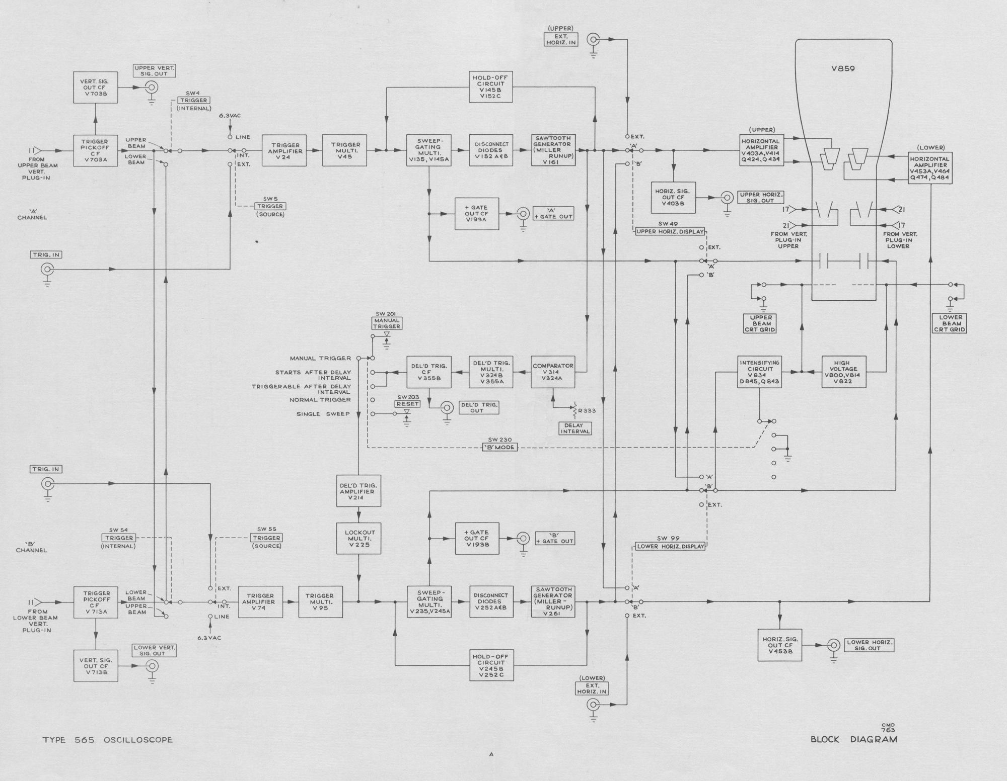
                   BLOCK DIAGRAM
A functional block diagram at the Type 565 Oscilloscope is shown in Fig. 3-1. The relationship of the circuits in each
block to those in other portions of the instrument is discussedin the detailed description of that circuit.

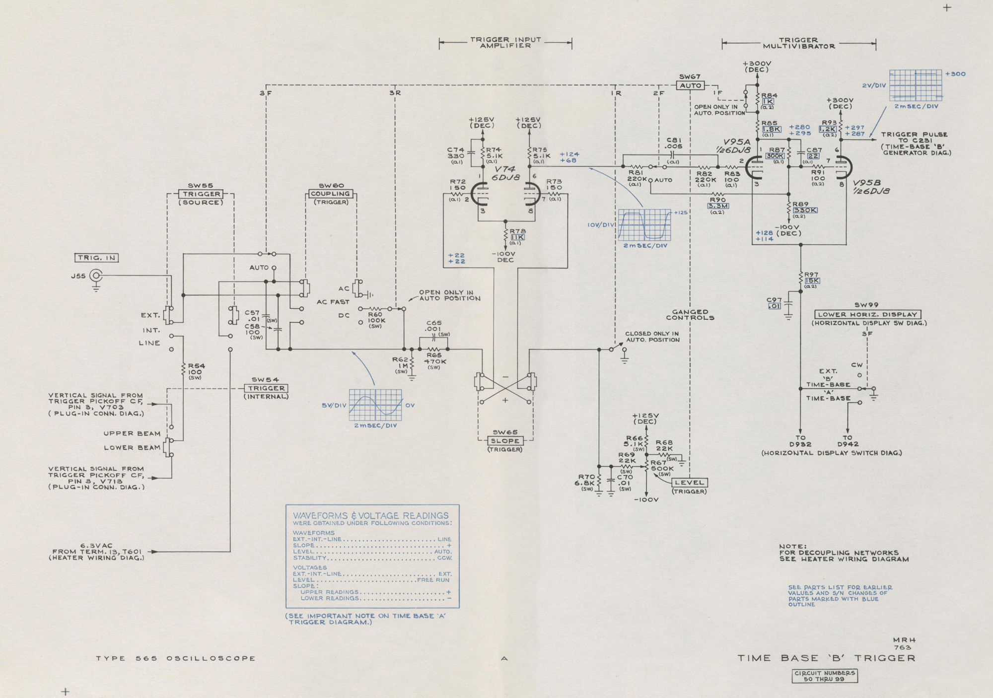
                    TIME BASE TRIGGER
General
Time Base ‘A’ Trigger and Time Base ‘B’ Trigger circuits are identical except for component reference numbers on
the schematics. The following circuit description pertains
to both circuits, but reference numbers for Time Base ‘A’
Trigger are used.
For best triggering stability, the Time Base Generator
requires a trigger pulse that is representative of the selected
triggering signal frequency, but otherwise consistent in
amplitude and wave-shape. Available triggering signals often vary in amplitude, waveshape, and frequency, and thus cannot be used directly to trigger the time base. The Trigger circuit is essentially a waveshaping circuit that converts a sample of the input signal into a pulse having a reasonably constant risetime and amplitude. Hence, frequency is the only variable characteristic remaining in the output trigger pulse.
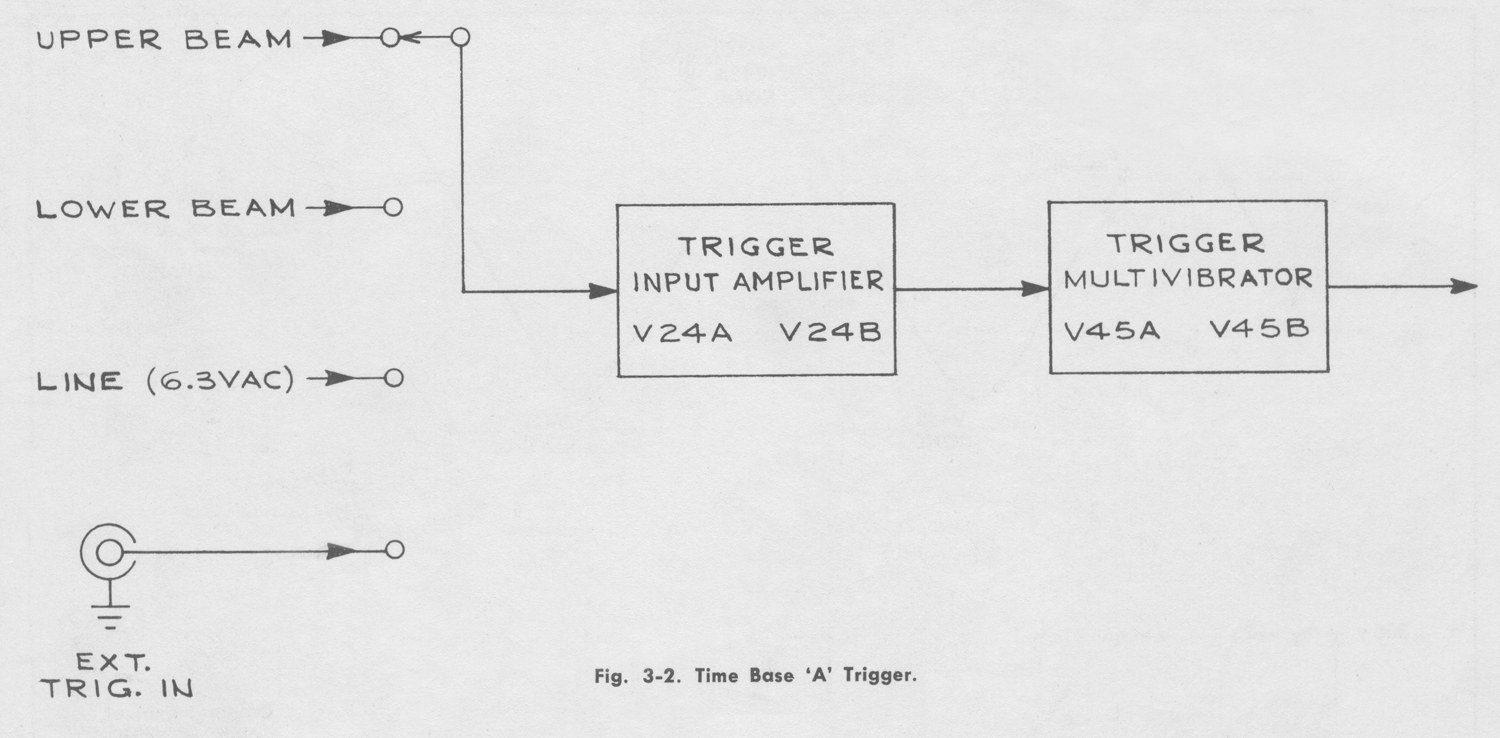
The block diagram, Fig. 3-2, shows the two basic elements
of the trigger circuit. The Trigger Input Amplifier amplifies
(and when desired, inverts) the incoming triggering signal and applies it to the input grid of the Trigger Multivibrator. The Trigger Multivibrator is essentially a switch that is either on or off, depending on the instantaneous voltage level at its input.  Its square wave output is applied to the Time Base Generator where it is differentiated to form positive and negative pulses. The negative pulses trigger the Time Base Generator while the positive pulses are clipped and not used.
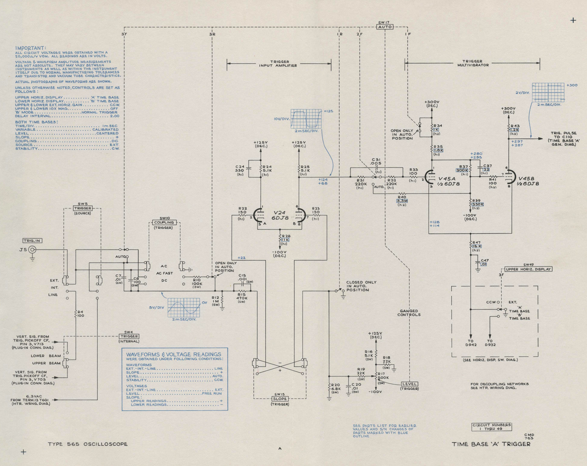
For the following description, refer to the Time Base ‘A’
Trigger schematic in the back of this manual.
Trigger Input Amplifier
The TRIGGER source switches are used to select the
appropriate trigger signal from one of four sources: upper beam vertical plug-in unit (UPPER BEAM), lower beam vertical plug-in unit (LOWER BEAM), TRIG. IN connector (EXT.), or line-frequency signal from the power transformer (LINE). Theselected signal is then applied to the COUPLING switch. (Information about the automatic mode, AUTO., of trigger operation is given later in this circuit description).
The COUPLING switch permits the operator to accept or
reject certain characteristics of the triggering signal. In the DC position, the coupling capacitors are shorted, coupling
both dc and ac signals to the Trigger Input Amplifier. In
the AC position, C7 and C8 in parallel are placed in the
signal path. An RC circuit consisting of C7-C8 and R12 is thus formed which blocks dc and attenuates ac signals below about 20 cycles. In the AC FAST position, C8 alone is placed in the signal path and R12 is placed in parallel with R10. This RC network blocks dc and rejects ac signals below 1000 cycles. The TRIGGER source and COUPLING switches are wired so the AC FAST function is bypassed when the LINE source is used.
The signal from the COUPLING switch is applied to the
SLOPE switch through R15-C15. (R15 and C15 prevent high amplitude positive signals from drawing excessive grid
current from V24.) The SLOPE switch determines whether or not the triggering signal will be inverted by the Trigger Input Amplifier. When the SLOPE switch is set to —, the signal is applied to the grid of  V24A and will not be inverted. For example, a positive-going signal at the grid of V24A will cause a positive-going change in the common cathode circuit. The fixed voltage at the grid of  V24B and the positive going change at its cathode reduce the current through V24B. This results in a positive-going change in plate voltage; hence, no inversion.
If the SLOPE switch is in the + position, the signal is applied to the grid of  V24B. In this case, V24B inverts the
signal in the manner characteristic of a single stage, plate-loaded amplifier.
The SLOPE switch also serves another function, it applies
a dc voltage from the LEVEL control to whichever grid of V24 is not connected to the COUPLING switch. (The need for this dc voltage is explained in the Trigger Multivibrator portion of this circuit description. At this point, however, the important consideration is the effect the dc voltage has on the amplified trigger signal at the plate of  V24B.)*
The voltage at the junction of R19 and R20 can be varied
between about +15 and -15 volts by adjusting the LEVEL
control. This voltage controls the average voltage at the plate of  V24B and the triggering signal either adds to or
subtracts from that average. Thus, in addition to being an
amplifier, the Trigger Input Amplifier is also a voltage
comparator. (V24 is a voltage comparator rather than a
difference amplifier since R24 and C24 balances the gain of V24A to that of V24B.)  This composite signal is applied to the input grid of the Trigger Multivibrator.
The Trigger Multivibrator is disabled unless R47 is grounded.
If the UPPER HORIZ. DISPLAY switch, LOWER HORIZ.
DISPLAY switch, or ‘B’ MODE switch is set for a function in which the operation of Time Base ‘A’ is required, then
R47 will be grounded.
Trigger Multivibrator
The Trigger Multivibrator, V45, is a typical bistable Schmitt
circuit. When the voltage at the grid of V45A is above a
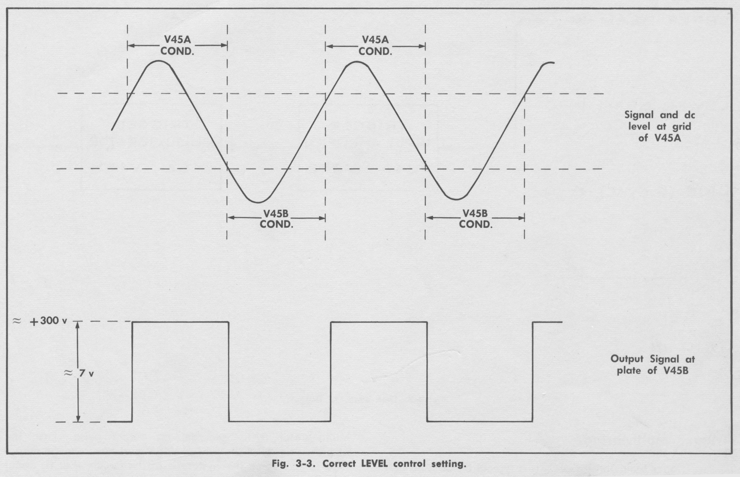
certain level, V45A conducts and V45B is cut off. In this state, the output voltage at the plate of  V45B is +300 volts. When the voltage at the grid of  V45A is below a certain level, V45B conducts and V45A is cutoff. The output voltage at the plate of  V45B is then about +293 volts. The transition from one state to the other occurs very rapidly, regardless of how slowly the input voltage passes the trip-level. Thus, the output of the Trigger Multivibrator is a square pulse of about 7 volts amplitude. The following example illustrates the sequence of events.
When a negative-going voltage change reaches about +111 volts at the input grid, the plate of  V45A rises and carries the grid of  V45B with it. V45B is driven into conduction (see Fig. 3-3). Since the cathode resistor R47 is common to both tubes, the conduction of  V45B tends to raise the
cathode voltage of  V45A. This further reduces the current
flow through V45A and compounds the original action of the input signal. V45A and V45B rapidly change conduction states; V45A cuts off and V45B conducts. The voltage at the plate of  V45B drops sharply. This voltage step is applied to a differentiating network in the Time Base Generator and becomes the negative-going trigger pulse required to start the time base action.

As the input signal continues into the positive-going portion of a cycle, the grid of  V45A rises beyond +111 volts to about +113 volts before the Trigger Multivibrator resets to its previous state. This approximate 2 volt difference in switching levels is the hysteresis range of the circuit.
As Fig. 3-3 and the previous description suggest, there are two basic requirements that must be met if the Trigger Multivibrator is to generate an output pulse. First, the
amplified signal at the grid of  V45A must have enough
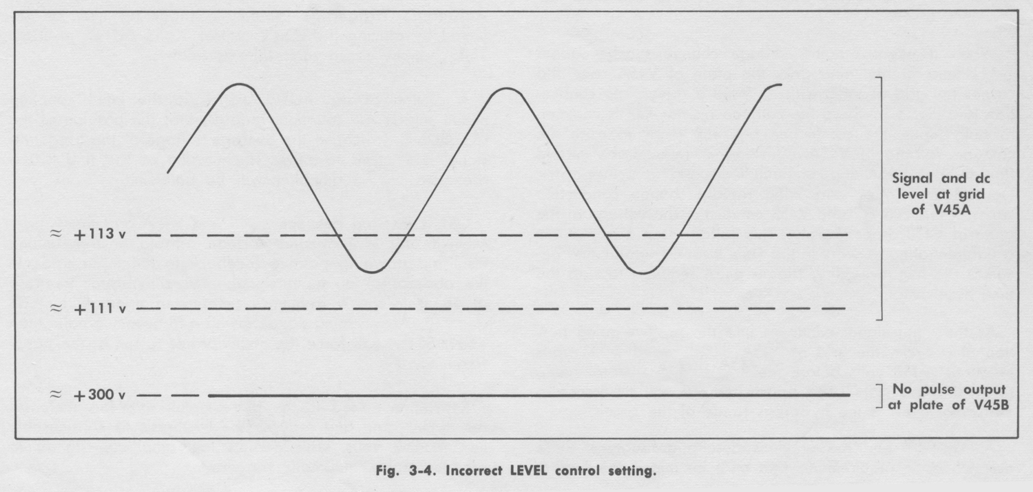
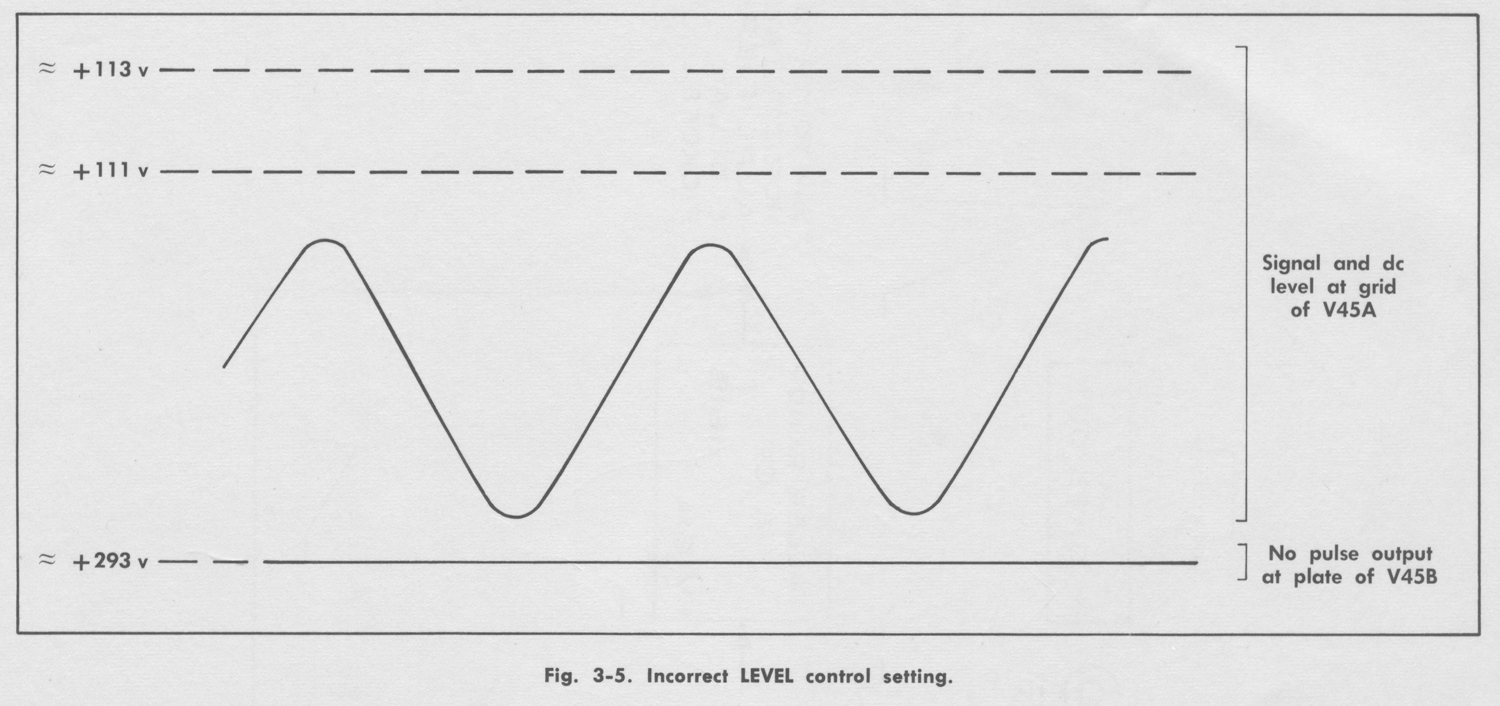
amplitude to overcome the hysteresis of the circuit; that is, about 2 volts peak to peak, or more. Second, the signal must be superimposed on a dc voltage that will permit it to cross the upper and lower hysteresis limits of the circuit; that is, about +111 volts and +113 volts. This second requirement is met through the use of the LEVEL control mentioned previously. Figures 3-4 and 3-5 illustrate the consequence of improper LEVEL control adjustment. In both cases, the signal amplitude is adequate to produce triggering, but the dc level of the signal is incorrect.
Automatic Triggering—Automatic triggering may be
selected by placing the LEVEL control in the AUTO. position.
This changes circuit operation as follows:
A section of the AUTO. switch in the input coupling circuit selects AC coupling, regardless of the position of the COUPLING switch, so the average voltage of the triggering signal is reduced to zero. The junction of  R19 and R20 is
grounded so the amplifier will be balanced. C31 is inserted between V24B and V45A and the Trigger Multivibrator is converted into an astable or free-running form by providing positive feedback to the input grid. In the absence of an input signal, the multivibrator free-runs at about 50 cps; a frequency determined primarily by C31 and R40. An incoming signal having a frequency greater than about 50 cps will force the multivibrator to run at the signal
frequency.
Resistance added in the plate circuit of  V45A increases the circuit gain and reduces the hysteresis to considerably less than 2 volts. This permits low amplitude signals to produce stable automatic triggering.

                    TIME BASE GENERATORS
The following description pertains to both time bases, but circuit reference numbers for Time Base ‘A’ are used.
The additional circuitry in Time Base ‘B’ is described in
a later portion of this section under the title “Time Base
‘B’ Lockout”.

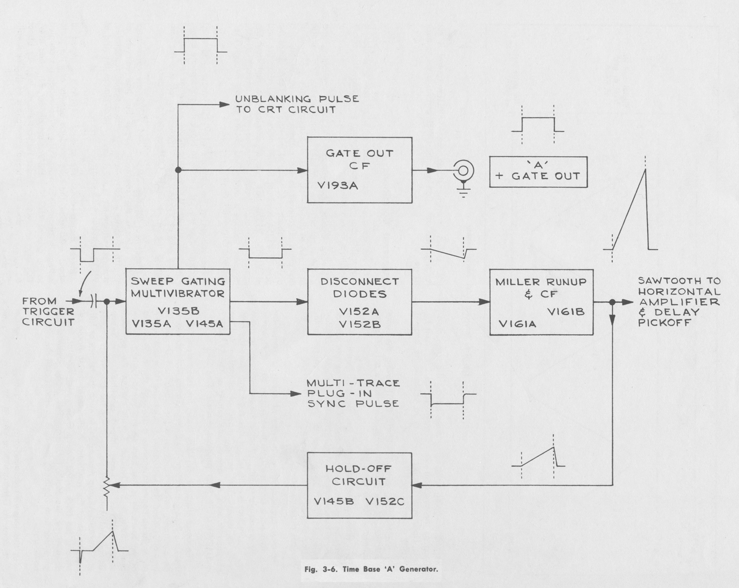
The Time Base Generator produces four output signals (see
Fig. 3-6):
1. a positive-going sawtooth which can be coupled to either or both horizontal amplifiers by the appropriate setting of the Horizontal Display switches. The sawtooth output is also permanently connected to the Delay Pickoff circuit (Time-Base ‘A’ only)
2. a positive-going unblanking pulse having the same duration as the sawtooth rise. Coupled to the Crt Circuit by
the Horizontal Display switches to unblank the beam(s)
being deflected by Time Base ‘A’.
3. a positive-going pulse (+ GATE OUT) having the same duration as the sawtooth rise. Coupled to a rear panel connector for external use.
4. a negative-going multi-trace sync pulse having the same
duration as the sawtooth rise. Coupled to the appropriate Vertical Plug-In Unit(s) by the Horizontal Display
switches. The trailing edge of the pulse causes multi-trace
plug-in units, operating in the alternate mode, to switch channels.
In most applications, each cycle of events is started by a trigger pulse from the Time Base Trigger circuit. However it is also possible to either disable the generator or to make it free run; that is—the end of one cycle will cause the next cycle to begin. The desired mode of operation will be
obtained through the appropriate setting of the STABILITY
and LEVEL (FREE RUN position) controls. (See Section 2.)
The block diagram, Fig. 3-6, shows the basic elements of
the Time Base Generator. The Sweep Gating Multivibrator is an electronic switch which turns the Disconnect Diodes on and off. When the Disconnect Diodes are back-biased, the Miller Runup begins to produce a sawtooth signal. A sample of the sawtooth is fed back to the Sweep Gating Multivibrator through the Holdoff Circuit. When the sawtooth sample reaches a predetermined amplitude, the Sweep Gating Multivibrator resets, switching the Disconnect Diodes.
The Miller Runup then resets, forming the retrace or falling
portion of the sawtooth. A sample of the sawtooth retrace is fed back to the Sweep Gating Multivibrator, but is delayed by the Holdoff Circuit. This delay prevents the generator from beginning the next sawtooth until the circuits have stabilized.
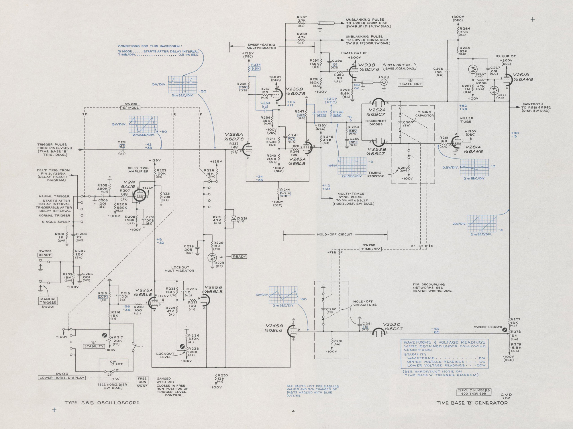
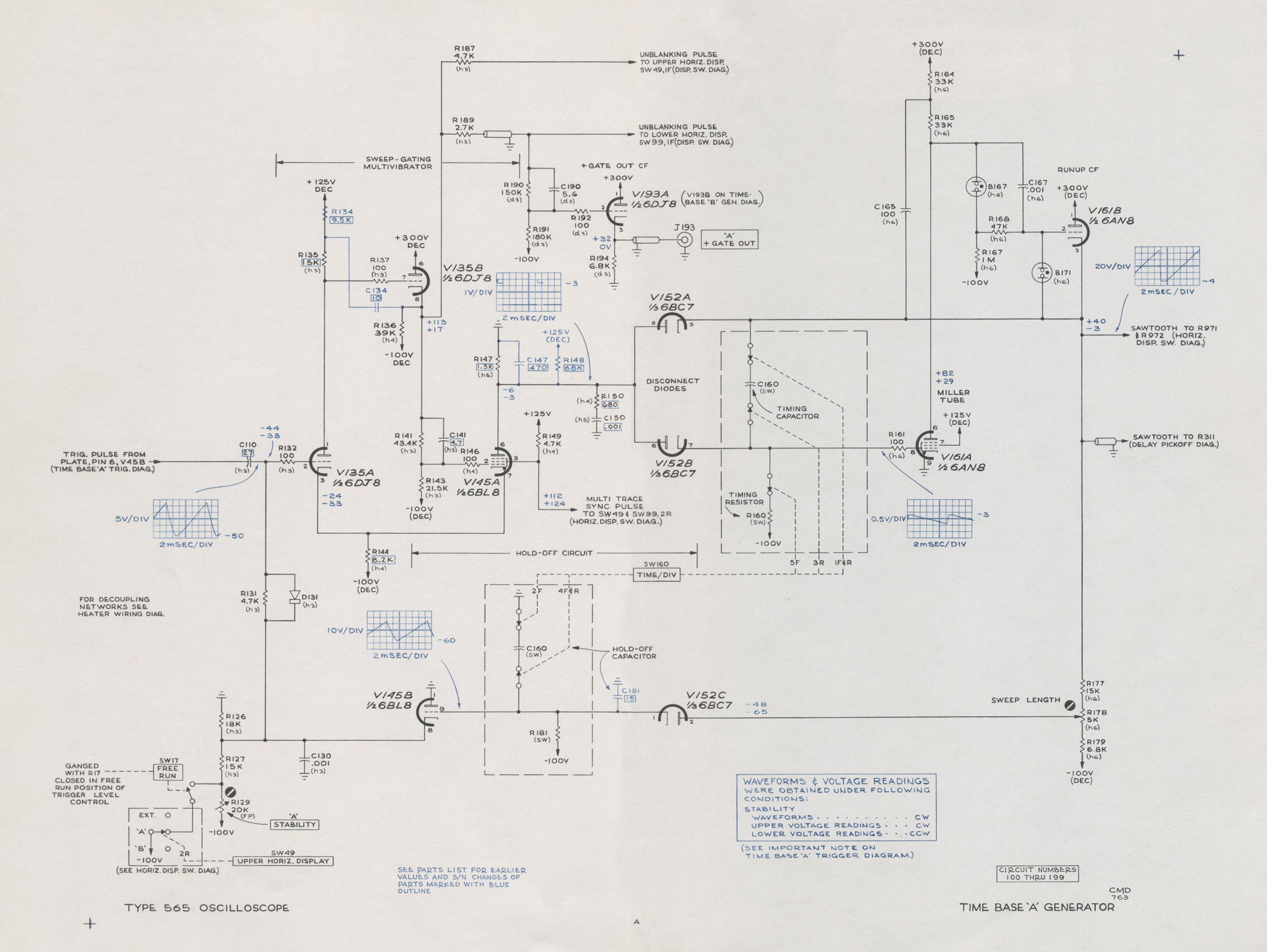
In the following detailed circuit description, refer to the
Time Base ‘A’ Generator schematic in the back of the manual.
Unless otherwise stated, the STABILITY control is set for triggered operation and the LEVEL control is set to mid- range.
Quiescent Conditions
In the quiescent state; that is, when the generator is
triggerable but no sweep is being generated, the circuit
conditions are as follows:
Sweep Gating Multivibrator—V135A is conducting and
V145A is cut off. The STABILITY control sets the grid voltage
of  V135A at about  -50 volts. The approximate +25 volts at
the plate is coupled to the cathode follower, V1358, and
divided to about -55 volts at the grid of  V145A. Since the grid of  V135A is about 5 volts more positive than the grid
of  V145A, V135A demands all available current from the
common cathode circuit. With no current through V145A,
its plate voltage is determined by the current through R147
and the disconnect diodes.
The voltage at the cathode at V135B (about +35 volts) is coupled to the Crt Circuit to blank the appropriate beam.
This same voltage is divided to about -25 volts and applied
to the grid of  V193A. Thus, V193A is cut off and the voltage at the ‘A’ + GATE OUT connector is zero.
Disconnect Diodes—V152A and V152B are conducting.
V152A clamps the sawtooth output bus (the cathode of
V161 B) at about -3.5 volts to provide a stable, repeatable,
starting voltage for the sawtooth. V152B clamps the grid of
V161A at about -2.5 volts.
Miller Runup—Since the grid of  V161A is clamped at
about -2.5 volts, the tube conducts heavily and the plate
voltage is about  +30 volts. The plate voltage is coupled to the grid of  V161B by the voltage divider, B167 and R167.
This type of voltage divider reduces the dc level by about
60 volts, but does not attenuate variations of the input voltage.
Hold-Off Circuit—V152C is conducting and V145B is cut off. The voltage divider network, R177, R178, and R179,
applies about -65 volts to the plate of  V152C. Thus V152C
conducts through R181 and sets the grid voltage of  V145B
at about  -65 volts. V145B is cut off since its cathode voltage is about  -50 volts; the same as the voltage at
the grid of V135A.
Cycle of Operation
When a negative-going pulse is received from the Trigger
Circuit at the grid of  V135A, the Sweep-Gating Multivibrator switches. Multivibrator action starts by V135A amplifying the trigger pulse. The positive-going pulse at the plate of  V135A is coupled to the grid of  V145A by the cathode follower, V135B. V145A is driven into conduction, causing a positive-going voltage change in the common cathode circuit. This is positive feedback to the cathode of  V135A which further reduces its conduction. Thus, the original action is compounded and the circuit rapidly switches.
V145A conducts and V135A is cut off. V145A conducts more heavily than did V135A. Therefore, the common cathode voltage is about  25 volts more positive than it was in the quiescent state, and V135A remains deep in cut off after the trigger pulse has ended.
When V135A cuts off, the voltage at the cathode of  V135B
rises sharply from about +25 to about +128 volts. This voltage step is coupled to the Crt Circuit and the + Gate Out Cathode Follower. The crt is thus unblanked and the beginning of the plus gate pulse is formed.
With V145A now in conduction, its plate voltage has
switched to a new level; about  -6 volts. This negative
voltage step cuts off conduction in the Disconnect Diodes.
The current through the timing resistor, R160, is now diverted and begins to charge the timing capacitor, C160. As the timing capacitor charges, the grid of  V161A goes negative.
The greatly amplified positive-going change at the plate of
V161A is coupled to the grid of  V161B through the neon
lamp, B167. The neon lamp lowers the dc level of the signal
by about  60 volts, but does not reduce the signal amplitude.
The cathode of  V161B provides the sawtooth output signal plus feedback to two points within the time base generator.
Feedback to the timing capacitor opposes the negative-
going change at the grid of  V161A. This action persists
throughout the period of the sawtooth and limits the total
change in grid voltage to less than one volt. Since the
voltage drop across the timing resistor is held nearly
constant, the current through the resistor is essentially a
constant value. This constant current flows into the timing
capacitor and the voltage across the capacitor increases at a very linear rate. The rate of rise of the sawtooth is a function of the RC time constant of the timing resistor and
capacitor.
An attenuated sample of the positive-going output sawtooth is applied to the plate of  V152C in the Hold-Off Circuit. The steady rise in voltage at the cathode of  V152C charges the hold-off capacitor while raising the grid voltage on V145B. When the sawtooth has reached about one-half
its final amplitude, V145B begins to conduct. As the sawtooth continues to rise, the cathode of  V145B and the grid of  V135A also rise. V135A will begin to conduct when its grid has risen about 20 volts. The plate voltage on V135A and the grid voltage on V145A drop and the cathode current no longer required by V145A is assumed by V135A. This positive feedback rapidly drives V135A into heavy conduction and V145A into cut off.
The negative-going voltage step at the cathode of  V135B
blanks the crt and forms the end of the + Gate Out pulse.
The positive going voltage step at the screen grid of  V145A is coupled to the appropriate vertical plug-in unit  to cause
a multi-trace plug-in unit, operating in the “alternate” mode, to switch channels.
When V145A cuts off, its plate voltage rises sharply to
about  -3 volts and brings V152B into conduction. The grid
voltage on V161A rises and its plate voltage drops, carrying the grid and cathode of  V161B with it. When the cathode of  V161B drops to about  -3.5 volts, V152A conducts to clamp the sawtooth output bus at that voltage level.
A sample of the falling voltage at the cathode of  V161B
is coupled to the plate of  V152C, cutting off its conduction.
While the hold-off capacitor was charged through the diode,
it must discharge through a large resistor, R181. This
retarded discharge (holdoff) delays the fall in voltage at the
grid (and hence, the cathode)  of  V145B. The STABILITY
control voltage divider network cuts off  V145B when its
cathode drops to about  -50 volts. Thus, V135A is reduced
from a stale of heavy conduction to its original quiescent
(triggerable) state.
Triggerable pulses which may arrive at the grid of  V135A
while the sweep is in progress have no effect since V135A
is already deep in cut off. When V135A is driven into heavy conduction at the peak of the sawtooth, trigger pulses still have no effect because their fixed amplitude is too low to bring V145A out of cut off. The Hold-Off Circuit extends this period of insensitivity and thus blocks the start of the
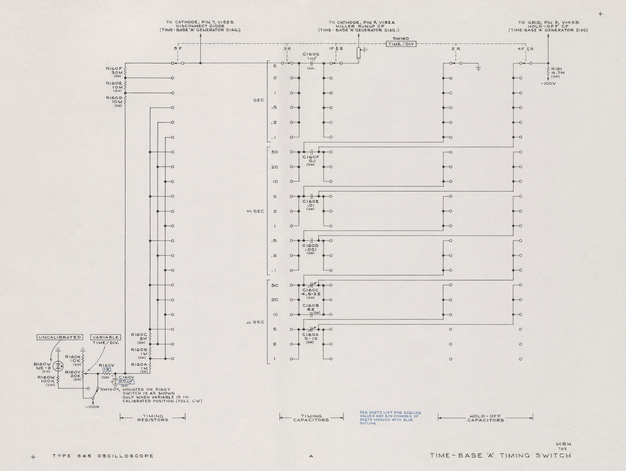
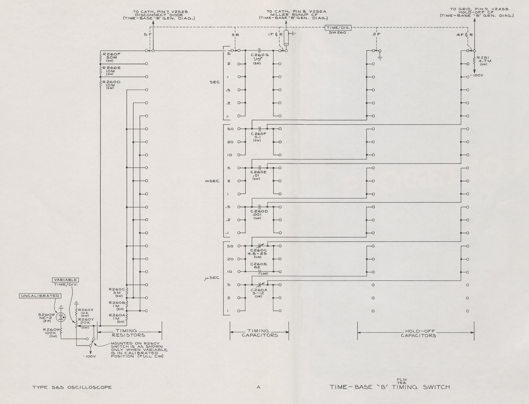
next cycle until the circuits have stabilized. Hold off time is required for stable triggering and is related to the timing capacitor being used. The proper holdoff capacitor is selected by the TIME/DIV. switch (see the Timing Switch
schematic).
Special Component Functions—C141 assures that the
Sweep-Gating Multivibrator will switch rapidly from one
conduction state to the other. R187 and R189 isolate the
shunt capacitance of the unblanking cables from the
Sweep-Gating Multivibrator so its switching speed is not degraded.
C165 aids V161B in charging the shunt capacitance in its
cathode circuit at the fastest sweep rates. C167 insures that the voltage divider consisting of B167 and R167 will have the proper frequency response. The SWEEP LENGTH control, R178, is set during calibration for the proper
sawtooth amplitude. D131 clips the positive-going portion of the triggering signal and C130 bypasses it to ground.

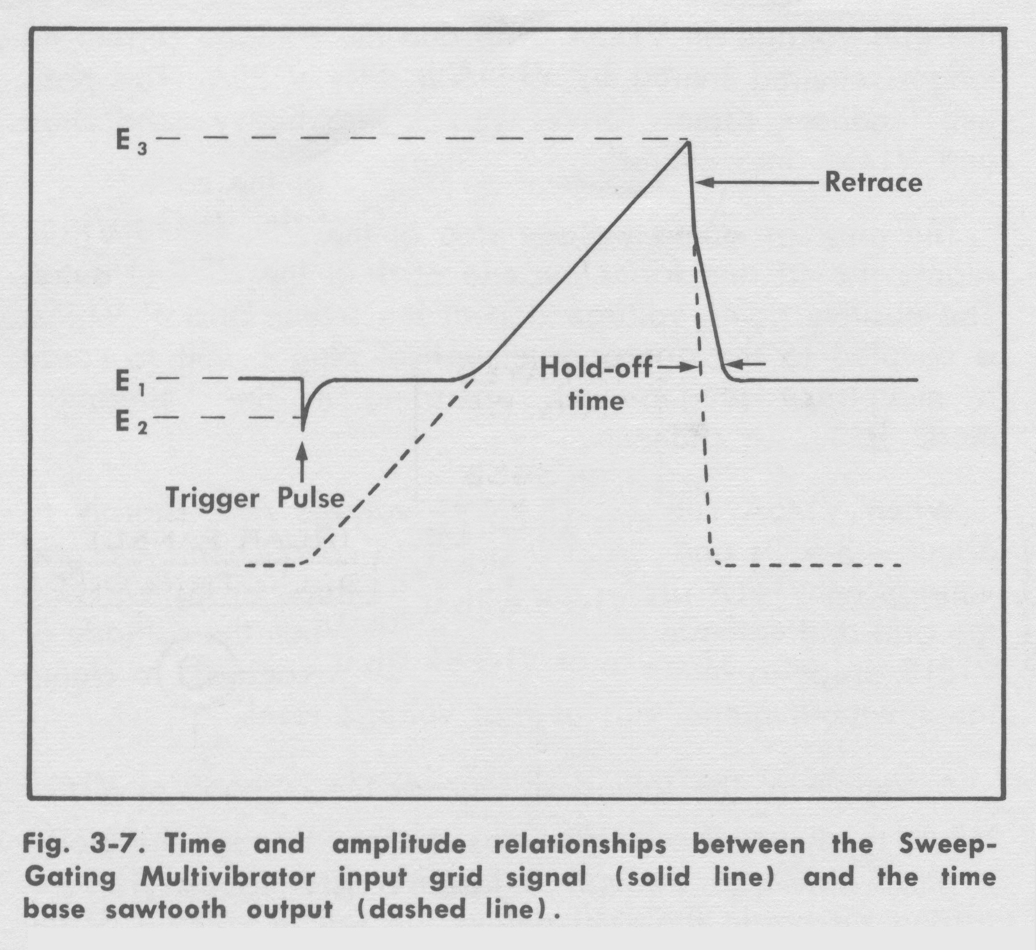
STABILITY control—Fig. 3-7 shows the relationship between the voltage at the Sweep-Gating Multivibrator input grid and the sawtooth output of the time base. Normally, the STABILITY control is set near mid-range so the voltage at the Sweep-Gating Multivibrator input grid will be at the level represented by E2 in Fig. 3-7. This voltage level is about 2 volts above the trip level (E1) required to cause the multivibrator to switch states. An incoming trigger from the Time Base Trigger circuit will drive the grid below the trip level.
The multivibrator will immediately switch states and a
sawtooth cycle will begin.
When the output sawtooth has reached about one-half of
its final amplitude, the Hold-Off Cathode Follower begins to conduct and raises the voltage on the Sweep-Gating Multivibrator input grid. The voltage continues to rise until it reaches the reset level represented by E3. At this level, the
multivibrator resets to its previous state and the retrace portion of the sawtooth begins. The falling voltage at the
input grid of V135A is retarded by the Hold-Off circuit, but
finally stabilizes at the quiescent level, E2. The entire circuit
is then ready for the next trigger pulse.
As you will note from the foregoing description and Fig. 3 7, the stability voltage at the Sweep Gating Multivibratar
input  grid must be at the correct level for triggered operation to occur. As the STABILITY control is turned
counterclockwise, the quiescent voltage will become more positive than E2. The amplitude of the trigger pulses will then be insufficient to drive the grid through the trip level E1. Sincethe time base will not operate, this condition is referred to as “lockout”.  As the STABILITY control is turned clockwise, the voltage becomes more negative than the trip level E2, and the Sweep-Gating Multivibrator will switch without waiting for a trigger pulse. As the sawtooth cycle thus initiatedcarries the input grid of the multivibrator through the retrace and hold-off period, the voltage will again fall below the trip level. Thus, another cycle will be initiated.
The sweep generation will repeat without the need for trigger pulses as long as the voltage from the STABILITY
control is sufficiently negative. This condition is referred to as ‘free run’ and can also be obtained by setting the LEVEL
control  to the FREE RUN position (provided UPPER HORIZ. DISPLAY is set to ‘A’ TIME BASE)».
§§§
Il testo prosegue nella settima parte.
Per consultare le altre schede dedicate a questo oscilloscopio esposto al museo MITI (su proposta di Fabio Panfili) scrivere “565” su Cerca.
Elaborazioni e testo a cura di Fabio Panfili.
Per ingrandire le immagini cliccare su di esse col tasto destro del mouse e scegliere tra le opzioni.


Oscilloscope Tektronix Type 565 serial 689, fifth part ( MITI Muesum)


Oscilloscopio Tektronix Type 565. Quinta parte.
Nell’inventario D del 1956 si trova al n° 3747 e risulta acquistato nell’agosto del 1964; vi si legge: “Silvestar ltd. Milano. Oscilloscopio Tektronix mod. 565 matr. 689. Dest. Elettronica ₤ 1·678·600”. Insieme alla fotocamera che è al n° 3746, dove si legge: “Silvestar ltd. Milano. Macchina fotografica Tektronix mod. C-12 completa di Bezel-Tektronix. Dest. Elettronica. ₤ 557·700”.
Il testo continua dalla quarta parte.
§§§
«DEMONSTRATION 1: Measuring time between two pulses, the first of which triggers Time Base ‘A’.
      Set the controls and switches on the instrument as listed above except as follows;
‘A’ TIME/DIV.                                            .1 mSEC
‘B’ TIME/DIV.                                              1 μSEC
Apply the Amplitude Calibrator signal to the input of both vertical plug-in units. The Upper Beam should display about one cycle of the squarewave signal.
Set the DELAY INTERVAL dial so the falling portion of
the squarewave  is intensified. Advance the Lower Beam
INTENSITY control to obtain a display of normal intensity.
The Lower Beam should now display a horizontally
expanded version of the signal in the intensified segment of the Upper Beam display.
Set DELAY INTERVAL so the Lower Beam trace starts at
About  the 50% amplitude level of the squarewave. Multiply the DELAY INTERVAL dial reading (e.g. 5.13) by the ‘A’ sweep rate. The product is the time duration of the
squarewave positive-going half-cycle.
Accuracy
Accuracy is determined by the combination of all the
following factors;
1. The basic accuracy of the Time Base Generator, and
therefore, of time measurements, is ±3%. In measurements
made directly from the crt, this means ±3% of full scale; that is, of the total time represented within the 10 major graticule divisions. However, when the measurement is made by using the sweep delay feature, the accuracy is ±3°/, of reading; that is, of the time being measured.
                          NOTE
During calibration, the internal DELAY START and DELAY STOP adjustments are set when the Time Base ‘A’ sweep rate is 1 mSEC per division. Therefore, delay measurements made when using the1 mSEC per division ‘A’ sweep rate will generally be most accurate. The delay accuracy obtained at any other ‘A’ sweep rate, 10 μseconds per division or slower, can be increased by calibrating
DELAY START and DELAY STOP at that sweep rate. (In so doing, you may wish to verify that all other ‘A’ sweep rates produce delays that are accurate within 3%). These adjustments do not affect the Time Base ‘A’ crt sweep rate. See the Calibration Procedure, Section 5, step 10.
2. The effect that the linearity of the Delay Interval system has on the measurement accuracy depends on the DELAY INTERVAL dial setting that is used. The linearity factor, as a percentage of reading, decreases as the dial setting increases. With any dial setting, the inaccuracy due to non-linearity will not exceed 0.5% of full scale delay.
3. Measurements are valid only when DELAY INTERVAL dial settings above 0.50 are used.
4. The triggering point can affect the measurement
accuracy since the triggering signal does not rise in zero
time. For example, if the sweep is triggered by the first
portion of the pulse rise, most of the pulse risetime will be
included in the measurement. This is of little concern in
measurements, such as the one made in Demonstration 1,
where the risetime of the signal is a relatively insignificant
percentage of the time being measured. However, as the
risetime percentage of the measured time increases, it
becomes more important that the triggering point be known.
One way to establish a known triggering point is to set the
LEVEL control at one end of the range in which a stable,
triggered Upper Beam display is obtained. Most of the
risetime of the signal will be included in the measurement
when:
a. ‘A’ TRIGGER SLOPE is set to + and LEVEL is set to
the — end of the “triggering” range (positive-going
signals), or
b. ‘A’ TRIGGER SLOPE is set to – and LEVEL is set to
the + end of the “triggering” range (negative-going signals).
5. The Time Base ‘A’ Trigger, Time Base ‘A’ Generator,
Delay Pickoff, and Time Base ‘B’ Generator circuits typically require a total of about 1.0 to 1.5 microseconds to respond to the signal event which triggers Time Base ‘A’. This small delay need not be considered unless it is a significant percentage of the time being measured. When necessary, add the circuit delay time to the measured time.
6. The 5, 2, and 1 μSEC/DIV A sweep rates generally are
not used for measurements such as those described in
Demonstration 1.
Summary—The method described in Demonstration 1 will
provide greatest time measurement accuracy when:
a. the internal DELAY START and DELAY STOP adjustments are calibrated at the sweep rate to be used,
b. dial settings above 4.0 or 5.0 are used,
c. the event triggering Time Base ‘A’ has a fast rise time,
and
d. Time Base ‘A’ sweep rates of 50 μSEC/DIV. or slower
are used.
DEMONSTRATION 2: Measuring time between two pulses of a pulse train, neither of which triggers Time Base ‘A’.
Set the controls and switches on the instrument as listed
except as follows:
‘A’ TIME/DIV.                                             .2 mSEC
Apply the Amplitude Calibrator signal to the input of  both vertical plug-in units. The Upper Beam should display about two cycles of the squarewave signal. Set the
DELAY INTERVAL dial so the squarewave rise located near the center of the Upper Beam display is intensified.
Advance the Lower Beam INTENSITY control to obtain
a display of normal intensity. The Lower Beam should now
display a horizontally expanded version of the intensified
Upper Beam display segment.
Set DELAY INTERVAL so the 50% amplitude level of the
squarewave rise intersects the vertical line at the center of the graticule. Note the exact DELAY INTERVAL dial setting (e.g. 5.14). Turn the DELAY INTERVAL dial clockwise until the 50% amplitude level of the squarewave fall intersects the same vertical graticule line used with the previous dial setting. Again note the exact DELAY INTERVAL dial setting.
Subtract the first dial setting from the second. The product of this difference and the Time Base ‘A’ TIME/DIV. equals the time duration of the squarewave positive-going half-cycle (between the 50% amplitude points).
Accuracy
Accuracy is determined by the combination of all the
following factors:
1. The basic accuracy of the Time Base ‘A’ generator is the same as described in Demonstration 1.
2. The percentage of error that the Delay Interval system linearity adds to the measurement depends on the numerical
difference between the two dial settings used; this error
decreases as the numerical difference increases. The amount of time error in the measurement is less than 1% of the full
scale delay (1%, of ten times the ‘A’ sweep TIME/DIV.).
However, this applies only when the DELAY INTERVAL dial settings are separated by at least 100 minor dial divisions.
NOTE
When the separation between dial settings is one hundred minor dial divisions or less, the desired time measurement can often be made more accurately by direct reading from a magnified crt display. See Demonstration 3; Magnification.
3. Measurements are valid only when DELAY INTERVAL
dial settings above 0.50 are used.
4. The accuracy of time measurements made according to Demonstration 2 is independent of the inherent circuit delays and of the triggering point (discussed in Demonstration 1), provided the ‘A’ LEVEL control setting is the same for each of the two dial readings.
5. The 2 and 1 μSEC/DIV. A sweep rates generally are not used in measurements such as those described in Demonstration 2.
Summary— The method described in Demonstration 2 can
provide a time measurement accuracy within 1% of reading.
 Accuracy will be greatest when:
a. the internal DELAY START and DELAY STOP
adjustments are calibrated at the sweep rate to be used, and
b.the numerical difference between the two DELAY INTERVAL dial settings is greatest.
DEMONSTRATION 3: Magnification
Complex signals often consist of a number of individual
events of different amplitudes. Since the trigger circuits
of the Type 565 are sensitive to signal amplitude, a stable
display will normally be obtained only when the sweep is triggered by the event having the greatest amplitude.
The “Starts After Delay Interval” mode permits the start of a sweep to be delayed for a selected time after the signal event having the greatest amplitude.  Any event within the series of events may then be displayed in magnified form as follows:
Set the controls and switches on the Type 565 as listed. Apply the Amplitude Calibrator signal to the input of both
vertical plug-in units. The Upper Beam should display
several cycles of the squarewave signal. Set the DELAY
INTERVAL dial to intensify one of the positive-going pulses.
Advance the Lower Beam INTENSITY control to obtain
a display of normal intensity. The Lower Beam display
should now contain the same signal information as the
intensified Upper Beam trace segment, but horizontally
expanded (magnified) ten times.
Increase the Time Base ‘B’ sweep rate to 1 microsecond
per division. Set the DELAY INTERVAL dial so the intensified segment in the Upper Beam trace extends throughout  the rise of one of the positive-going pulses. The Lower Beam display now gives X1000 magnification.
Slowly turn the DELAY INTERVAL dial. Note that any
portion of the Upper Beam display can be brought into view in magnified form on the Lower Beam display (except for a small portion at the beginning and end of the Upper Beam Display). The DELAY INTERVAL dial indication corresponds to the number of major graticule divisions
between the beginning of the Upper Beam trace and the
beginning of the intensified trace segment; e.g. 7.00 = 7
major divisions.
Set the Time Base ‘B’ sweep rate to 10 microseconds per division. Set the DELAY INTERVAL dial so a squarewave
rise is centered in the Lower Beam display. Set UPPER
HORIZ. DISPLAY to ‘B’ TIME BASE and turn on the Upper Beam IOX MAG. Set the Upper Beam horizontal POSITION so the squarewave rise is visible in the Upper Beam display.
The Lower Beam now gives 100 times magnification
and the Upper Beam gives 1000 times magnification of the
information that was contained in the intensified segment of the original Upper Beam display.
Both the Upper and Lower Beam display will probably
exhibit some horizontal jitter. Part of the jitter is due to a
slight inconsistency in the Amplitude Calibrated signal
frequency, and part is due to jitter in the delay system. The jitter contributed by the delay system is less than 0.05%
of the Time Base ‘A‘ sweep rate (0.05% of 1 millisecond
= 0.5 microsecond). With 1000 times magnification, the
Upper Beam sweep rate is 1 microsecond per division.
Hence, the jitter due to the delay system is less than one-half major division.
Accuracy
1. The accuracy of time measurements made from
magnified displays such as those described in the foregoing
para
graphs, depend solely on the Time Base ‘B‘ sweep rate
accuracy (±3%, with the 10X MAG. off and ±5 with the10X MAG. on).
DEMONSTRATION 4: Delayed Trigger
Ordinarily, a signal which is to be displayed is also used to trigger the oscilloscope sweeps so a stable display is obtained. In some situations, it may be desirable to reverse this situation. The sweep-related output pulses, available at the rear panel of the Type 565, can be used* as the input or triggering signals for external devices. The output signal of the external device will then produce a stable display while the oscilloscope sweep free-runs.
To demonstrate one method of performing this operation,
proceed as follows:
Set the controls and switches on the Type 565 as listed
except as follows;
‘A’ TRIGGER source                                    EXT.
‘A’ TRIGGER COUPLING                          DC
‘A’ TIME/DIV.                                              10 μSEC
‘B’ MODE                                                     NORMAL TRIGGER
‘B’ TRIGGER LEVEL                                  FREE RUN
DELAY INTERVAL                                      1.00
INTENSITY (Upper)                                     normal
Connect: (rear panel and front panel connections)
‘B’ + GATE OUT              to                         ‘A’ TRIG. IN
DEL’D TRIG. OUT             to      INPUT of the Upper Beam plug-in unit
Set ‘A’ TRIGGER LEVEL mid-way between ‘O’ and FREE
RUN so Time Base ‘A’ triggers on the rise of the ‘B’ + GATE
OUT signal. The Upper Beam should now display a narrow,
positive-going pulse.


*Output current must not exceed 2 ma peak.

The oscilloscope display that you have established shows a pulse that is available from the Type 565 during each Time Base ‘A’ sweep. In a practical application, the pulse would
not be applied to the vertical input of the oscilloscope, but
instead to some external device to be tested. The pulse would serve as the trigger pulse for the external device and the output of the device would be displayed on the oscilloscope.
Since the pulse has a known time-relationship to
each Time Base ‘A’ sweep, the output of the device will
provide a stable display on the oscilloscope, as though the oscilloscope were triggered in the normal manner.
The set-up described in the foregoing paragraphs permits you to vary the repetition rate of the pulse applied to the
external device. To do this, monitor the pulse signal on another oscilloscope and set ‘B’ TIME/DIV. and VARIABLE for the desired repetition rate. ‘A’ TIME/DIV. controls only the display sweep rate as long as the Time Base ‘A’ Sweep rate is at least twice that of Time Base ‘B’.
Set ‘B’ MODE to MANUAL TRIGGER and press the MANUAL TRIGGER push-button. This set-up permits you to produce each DEL’D TRIG. OUT pulse manually.
DEMONSTRATION 5: Pulse Generation The ‘B’ + GATE OUT signal of the Type 565 can be used as a low-current*, variable repetition rate, variable dutyfactor pulse generator in applications where the pulse shape is of secondary importance. To use the Type 565 in this manner, proceed as follows:
Set
UPPER HORIZ. DISPLAY                      ‘A’ TIME BASE
LOWER HORIZ. DISPLAY                     ‘B’ TIME BASE
‘B’ MODE                   STARTS AFTER DELAY INTERVAL
DELAY INTERVAL                                   about 0.50
LEVEL  (‘A’ and ‘B’)                                  FREE RUN
The pulse signal is available at the ‘B’ + GATE OUT
connector on the rear panel. Monitor the signal on another
oscilloscope and establish the desired pulse repetition rate by setting the Type 565 ‘A’ TIME/DIV. and VARIABLE. Establish the desired duty factor by setting ‘B’ TIME/DIV.
The maximum pulse repetition frequency that can be
obtained in this manner is about 10 to 12 kc. Maximum duty factor is about 0.6, decreasing with faster sweep rates.
A slight alteration in this set-up will produce a double- pulse generator. To do this, start with a B sweep rate that is
at least 5 times faster than the A sweep rate. Set DELAY
INTERVAL to about 5.00. Connect a 100 pf capacitor between the center conductors of the A+ GATE OUT and DEL’D TRIG OUT connectors on the rear of the instrument.
The B + GATE OUT pulse will now occur twice during each A sweep; the first beginning as A sweep begins and
the second begins at the end of the delay interval.
The time separation between pulses is controlled by setting
DELAY INTERVAL. The minimum separation that can obtained is a function of the Time Base B Generator hold-off time.


*Output current must not exceed 2ma peak.

Triggerable After Delay Interval
Complex signals often contain a number of individual
events of different amplitudes. Since the trigger circuits in the Type 565 are sensitive to signal amplitude, a stable display will normally be obtained only when the sweep is
triggered by the event having the greatest amplitude.
The TRIGGERABLE AFTER DELAY INTERVAL feature of the Type 565 provides a means of triggering the sweep by events other than those having the greatest amplitude. The following instructions permit you to demonstrate that Time Base ‘B’ can be triggered by virtually any event within a series of events.
Set the controls and switches on the instrument as listed
except as follows:
Lower Beam INTENSITY                  for normal display
Time Base ‘B’ TRIGGER  controls.      some settings as Time controls Base ‘A’ TRIGGER
Connect the CAL. OUT signal to both the Upper and Lower
Beam vertical input connectors. Each beam should present
a square wave display.
Turn the DELAY INTERVAL dial about 2 turns in either
direction. Notice that both the Lower Beam display and
the brightened segment in the Upper Beam display, move
smoothly across the crt.
Set the DELAY INTERVAL dial so the brightened segment
in the Upper Beam display begins about in the middle of a
pulse top. Notice that the Lower Beam display also begins
in the middle of a pulse top. Now, set the ‘B’ MODE switch
to the TRIGGERABLE AFTER DELAY INTERVAL position.
Notice that the brightened segment in the Upper Beam
display has shifted to the next pulse on the right. The Lower
Beam display now begins within the rising portion of the pulse.
Now turn the DELAY INTERVAL dial several full turns.
The brightened segment in the Upper Beam display should
jump from one pulse to the next. In this demonstration,
the Lower Beam display appears unchanged because all
pulses are identical.
The display is produced in the following manner:
Time Base ‘B’ produces one sweep for each ‘A’ sweep.
‘B’ sweep will begin at some time after the start of  ‘A’
sweep. This time is the total of (1) the Time Base ‘A’ sweep
rate (TIME/DIV.) multiplied by the DELAY INTERVAL dial setting, plus (2) the time between the end of this delay
interval and the next event in the signal which can trigger Time Base ‘B’.
It is possible that Time Base ‘B’ might not be triggered
until long after Time Base ‘A’ has completed its sweep. If
separate triggering signals are being applied to the two time
bases, Time Base ‘A’ could produce several additional sweeps
before Time Base ‘B’ receives a triggering signal. Because
of this, the brightened trace segment could appear at any
point on the Upper Beam trace or might not appear at all.
Delayed Trigger Output
The delayed trigger output pulse is always available at the rear panel connector at the predetermined time during each sawtooth produced by Time Base ‘A’, regardless of the ‘B’ MODE switch setting. This output signal is discussed in greater detail under “Starts After Delay lnterval”, Demonstration 4.
External Horizontal Inputs
For special applications, you can deflect either beam horizontally with an externally derived signal. This permits you to use the oscilloscope to plot one function versus
another. The maximum bandpass of the horizontal amplifier
occurs at the fully clockwise setting of the EXT. HORIZ. GAIN control; dc to at least 350 kc.
To use an external signal for horizontal deflection, connect the signal to either the Upper or Lower Beam EXT. HORIZ. IN connector. Place the appropriate horizontal display switch in the EXT. position. The horizontal deflection factors can be varied by adjusting the EXT. HORIZ GAIN
control such that a one volt peak-to-peak signal will produce from zero to at least 10 major graticule divisions of deflection.
The 10X MAG. switch has no effect when external horizontal deflection is used.
Amplitude Calibrator
The amplitude calibrator provides a convenient source of square waves of known amplitude at a frequency of approximately 1kc. The square waves are used primarily to adjust probe compensation and to verify the amplitude calibration of the oscilloscope vertical deflection systems.
Calibrator square waves are adjustable from 1 millivolt to 100 volts, peak-to-peak, in decade steps. The amplitude is controlled by the setting of the PEAK-TO-PEAK VOLTS switch. The output voltage is ac-curate within 3% of the PEAK- TO-PEAK VOLTS switch setting when the output is connected to a high-impedance load such as the INPUT connector of a vertical plug-in unit.
When the .001, .01, .1 volt settings of the PEAK-TO-PEAK
VOLTS switch are used, it will be necessary to use a coax
cable to take the signal from the CAL. OUT connector. The
outer conductor of the cable must make good contact with
the shield portion of the CAL. OUT connector in order to
obtain an accurate output voltage.
              AUXILIARY FUNCTIONS
Intensity Modulation
The rear panel jacks marked UPPER BEAM CRT GRID and LOWER BEAM CRT GRID permit external signals to vary the intensity of the traces (Z-axis modulation). This feature can be used to refer oscilloscope time measurements to an external timing standard.
In some applications, you may wish to use the VARIABLE
TIME/DIV. control at an uncalibrated position to obtain a
sweep rate other than those provided by the TIME/DIV.
switch. Intensity modulation with time-marker pulses will
permit you to establish and monitor the desired sweep rate.
This will eliminate the need for a separate vertical display of a time reference signal.
Fast-rise pulses of short duration are usually used for
intensity modulation because they produce an easily
interpreted display. When other types of signals are used, it is important to note that sinewaves below 250 cycles will be
attenuated due to the ac signal coupling within the
instrument. The signal amplitude required for visible trace
modulation depends upon the intensity level of the
unmodulated trace.
Trace Photography
Several features of the Type 565 Oscilloscope are
particularly important when photographying  the crt display. The rubber washers normally installed between the graticule and the bezel should be removed when either the light filter or a camera-mount bezel is installed. When a light filter is used, the graticule should be placed between it and the crt.
There are two pairs of holes in the graticule for the scale
illumination pilot lamps. One pair is colored red and will
produce red graticule lines when aligned with the pilot lamps.
The second pair is clear and will produce white graticule
lines. White lines should be used whenever the light filter
is installed or when photographs are being taken. When the
trace is viewed without a light filter, the red lines are usually easier to see. In all cases, the side of the graticule that bears the scribed lines should be placed against the crt face.
The CONTRAST control, located inside the instrument at
the left side of the High Voltage Power Supply chassis, permits you to control the relative intensity of the intensified trace segment obtained in delayed sweep operation. This control is usually set fully clockwise (greatest contrast) for normal viewing. However, it may require resetting for less contrast while photographs are being taken so all portions of the picture will be properly exposed.
The CAMERA POWER jack, on the front panel, provides a
convenient power source for future camera accessories.
The Single-Sweep feature, described previously in this
section, is often used when non-repetitive waveforms are photographed.
Aux. Power Jack
The auxiliary power jack on the rear panel is provided to
power future accessories for the Type 565, as well as other devices».
§§§
Il testo prosegue nella sesta parte.
Per consultare le altre schede dedicate a questo oscilloscopio esposto al Museo MITI (su proposta di Fabio Panfili) scrivere “565” su Cerca.
Elaborazioni e testo a cura di Fabio Panfili.
Per ingrandire le immagini cliccare su di esse col tasto destro del mouse e scegliere tra le opzioni.
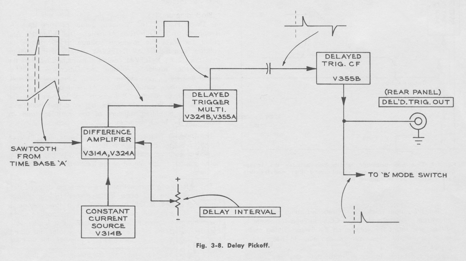


Oscilloscope Tektronix Type 565 serial 689, fourth part ( MITI Museum)


Oscilloscopio Tektronix Type 565 serial 689. Quarta parte.
Nell’inventario D del 1956 si trova al n° 3747 e risulta acquistato nell’agosto del 1964; vi si legge: “Silvestar ltd. Milano. Oscilloscopio Tektronix mod. 565 matr 689. Dest. Elettronica ₤ 1·678·600”. Insieme alla fotocamera che è al n° 3746, dove si legge: “Silvestar ltd. Milano. Macchina fotografica Tektronix mod. C-12 completa di Bezel-Tektronix. Dest. Elettronica. ₤ 557·700”.
Il testo continua dalla terza parte.
§§§

                       «SECTION 2
         OPERATING INFORMATION

 Introduction
This portion of the manual contains general information about the many features of the Type 565 and specific information about the use of each control. The information
is intended to help you gain full use of the potentialities of
the instrument.
       BRIEF DESCRIPTIONS OF CONTROL AND
                     SWITCH FUNCTIONS
                             NOTE
More complete descriptions of the controls and switches and how to use them is included in the latter portion of this section.
                      UPPER BEAM
These controls and switches are located on the left half of the front panel and affect the upper beam display.
UPPER HORIZ. DISPLAY
(Upper Horizontal Display)  Provides
selection between ‘A’ TIME BASE, ‘B’ TIME BASE, and EXT. [external] signal sources  for horizontal deflection of the upper beam.
EXT. HORIZ. GAIN
(External Horizontal Gain) Functions only
when the UPPER HORIZ. DISPLAY switch is in the EXT. position. Permits variation of the external horizontal input deflection sensitivity to a maximum of about 0.1 volt per division.
POSITION (Upper Beam)
(Not part of Time Base ‘A’) Used to move
the display horizontally. This is a combination coarse and vernier control. About 55° vernier adjustment is available at any position of the control.
10X MAG.     (Ten-Times Magnifier) Expands a one major division segment of the display to ten times normal width. The segment of the normal display which was positioned at the center of the crt will be displayed. When the 10X MAG. is used, the sweep rate is ten times faster than indicated by the TIME/DIV. switch. 10X MAG. has no effect when an external horizontal input is used.
FOCUS          Adjust in conjunction with the ASTIG. control to obtain sharpest possible trace definition.
ASTIG.         (Astigmatism) Adjusted so the FOCUS control can be set for equally sharp definition of both the horizontal and vertical portions  of the display.
INTENSITY         Allows variation of trace brightness.
                          LOWER BEAM
These controls and switches are located on the right half of
the front panel. They are identical in function to those provided for the upper beam display, but affect only the lower beam display.
                           TIME BASE ‘A’
These controls and switches are located on the left half of
the front panel and affect only Time-Base ‘A’.
TRIGGER
(UPPER BEAM)  (LOWER BEAM)     Functions only when the EXT.-INT.-LINE switch is in the INT. position. Selects between the Upper Beam and Lower Beam vertical channel signals as the source of  triggering signal.
EXT.-INT.-LINE     (External-Internal-Line) Provides a selection of triggering signal sources: external (EXT.) from TRIG. IN connector; internal lNT.) from either Upper or Lower Beam vertical  channel, or a sample of the power line waveform (LINE)
COUPLING            Allows acceptance or rejection of some
(AC-AC FAST- DC)  characteristics of triggering signals. AC rejects dc and very low frequency ac signals. AC FAST rejects signals below about 1 kc. DC accepts all frequencies and dc.
SLOPE (+ -)      Determines whether the sweep will trigger on the positive-going or negative-going portion of a signal.
LEVEL (AUTO.-FREE  RUN)    A three function control. Except at the extreme clockwise and counterclockwise positions, it operates as a triggering LEVEL control. LEVEL selects the amplitude point on the triggering signal at which the sweep will trigger. AUTO. (automatic) overrides the function of the COUPLING switch and LEVEL control and selects AC coupling and ‘0’ level. In the absence of a triggering signal, a reference trace is displayed on the crt (about 50 sweeps per second, maximum). The FREE RUN position provides recurrent sweeps at a rate depending upon the TIME/DIV. switch  setting (about 12,000 sweeps per second at one microsecond per division).
STABILITY     A screwdriver adjustment which sets the time-base generator susceptibility to pulses from the trigger circuits.
TIME/DIV.     (Time Per Division) Selects the rate at which the spot moves across the crt.
VARIABLE      An uncalibrated control which provides sweep rates other than those included on the TIME/DIV. switch. Rates to less than 0.4 of that indicated by the TIME/DIV. switch can be obtained.
DELAY INTERVAL    (‘A’ Time Per Division Multiplied by a figure between one and ten). Used with ‘A’ TIME/DIV. switch to determine the delay interval between the start of ‘A’ sweep and the delayed trigger pulse. This pulse is fed to a rear-panel output connector and to the ‘B’ MODE switch. With the proper setting of the ‘B’ MODE switch, this pulse can either; (1) start ‘B’ sweep (STARTS AFTER DELAY INTERVAL) or (2) make ‘B’ sweep susceptible to trigger pulses (TRIGGERABLE AFTER DELAY INTERVAL).
                                      TIME BASE ‘B’
These controls and switches are located on the right half
of the front panel and are identical to those for Time-Base
‘A’ with the addition of the following:
‘B’ MODE     Selects the type of operation that Time Base ‘B’ will perform. In the NORMAL TRIGGER position, the operation is identical to that of Time Base ‘A’. TRIGGERABLE AFTER DELAY INTERVAL and STARTS AFTER DELAY INTERVAL are explained  previously under “DELAY INTERVAL”.
MANUAL TRIGGER and SINGLE SWEEP
function as follows:
MANUAL  TRIGGER        Overrides all TIME BASE ‘B’ TRIGGER controls. The spot will sweep across the crt once each time the MANUAL TRIGGER button is pushed.
SINGLE SWEEP           Permits Time Base ‘B’ to move the spot across the crt once each time the SINGLE SWEEP button is pushed. Pushing the button does not start the sweep; it permits the trigger circuit to do so.
                      AMPLITUDE CALIBRATOR
PEAK-TO-PEAK   VOLTS        Selects output voltage delivered to the CAL. OUT connector from the available decade steps, .001 volt to 100 volts. It also permits turning off the Amplitude Calibrator.
                              OTHER CONTROLS
TRACE ALIGNMENT        Used to rotate the crt display to coincide with the graticule markings.
SCALE ILLUM                (Scale Illumination) Adjusts the brightness of the graticule markings.
POWER ON                     Ac line switch.
                    FIRST-TIME OPERATION
The following information is intended to help you prepare your Type 565 Oscilloscope for first-time use. It is also suggested that a quick-check, similar to these steps, be performed each day before beginning measurements.
Whenever plug-in units are exchanged, steps 10 and 11
must be checked.
1. Install any general-purpose amplifier plug-in units (e.g. 3A1, 3A2, 2A60, 2A63, 3A75, 3A72, 3A74, etc.).
2. Set Upper and Lower Beam display controls and switches as follows:
INTENSITY                  counterclockwise
POSITION (horiz.)        centered
10X MAG.                     off (pushed in)
UPPER HORIZ. DISPLAY       ‘A’ TIME BASE
LOWER HORIZ. DISPLAY       ‘B‘ TIME BASE
3. Set the applicable controls and switches on both vertical
plug-in units as follows:
VOLTS/DIV.                     5
VARIABLE                       CALIBRATED
AC-DC-GND.                   AC
POSITION (vert.)             centered
4. Set TIME BASE ‘A’ and TIME BASE ‘B’ controls and
switches as follows:
TIME/DIV.                        .2 mSEC
VARIABLE                        CALIBRATED
LlNE—lNT.—EXT.           LINE
LEVEL                               AUTO.
STABILITY                       clockwise (screwdriver adjustment)
5. Set the remaining controls and switches as follows:
‘B’ MODE                          NORMAL TRIGGER
PEAK-TO-PEAK VOLTS            10
                              NOTE
Controls not mentioned may be left in any position.
6. Connect the power cord to the proper voltage source
and turn on instrument power.
7. Allow several minutes for the instrument to warm-up.
Then, slowly advance the INTENSITY controls to obtain
traces of moderate brightness. It may be necessary to
readjust the vertical POSITION controls.
8.Slowly turn the Time Base ‘A’ STABILITY control
counter-clockwise. The upper beam trace should dim and then
disappear. Set the STABILITY control in the middle of the
“dim” range. Adjust the Time Base ‘B’ STABILITY control
in the same manner.
NOTE
This setting of the STABILITY control is correct for most applications. However, when the triggering signal frequency is above approximately one megacycle, it may be necessary to make a slight readjustment to obtain a completely stable display.
9. Connect the CAL. OUT signal to the INPUT connector of both vertical plug-in units. Set the LINE—INT.— EXT. switch in both time-base blocks to INT. Adjust the
INTENSITY controls so the vertical lines in the square wave display are just visible.
10. Adjust the FOCUS controls so the vertical and horizontal portions of each display are equally focused. Then adjust the ASTIG. controls for best focus in the horizontal and vertical portions of each display. Repeat the
adjustments, if necessary, until no further improvement can be made.
                             NOTE
It may be necessary to touch-up the FOCUS control adjustment whenever a major change is made in the INTENSITY control setting. In some applications, such as those involving low repetition rate signals displayed at fast sweep rates, a very dim display will be obtained. Since better display focus can be obtained when the INTENSITY
control is set below maximum, you may wish to use a moderate INTENSITY control setting and a viewing hood. The viewing hood will block external light and make dim displays useable.
11. Use a screw driver to set the gain adjustment on the front panel of the plug-in units so each of the square wave displays is exactly 2 major divisions in amplitude.
If you require additional information about this adjustment, see the manual for your particular plug-in unit.
12. Remove the signal input leads. Turn both trigger LEVEL controls fully clockwise. The traces should be parallel to the horizontal  graticule lines. If not, adjust the TRACE ALIGNMENT control to remove any tilt.                    NOTE
The TRACE ALIGNMENT control is a screw-driver-
adjustment located on the front panel just below the crt. This control permits the operator to easily offset any trace tilt introduced by the earth’s magnetic field.
When the preceding steps have been completed, the
Type 565 Oscilloscope is ready for use.
NOTE
It is important that steps 10 and 11 be rechecked each time plug-in units are exchanged in the Type 565.
         USING THE TYPE 565
Signal Input Connections
Signals to be displayed on the oscilloscope are connected to the input connectors of the vertical plug-in units.
The signals within the plug-in unit are then changed to the
proper amplitude and used to produce vertical deflection
of the electron beams. It is frequently possible to make the
input connections with unshielded test leads. This is
particularly true when you are observing a high-level, low-frequency signal from a low impedance source. When test
leads are used, place a ground connection between the
oscilloscope chassis and the output “common” terminal of
the signal source.
In many applications, unshielded leads are unsatisfactory
for making input connections due to the noise pickup
resulting from stray magnetic fields. In such cases, shielded
cables should be used. The ground conductors of the cable
must be connected to the chassis of the oscilloscope and
the output  “common” terminal of the signal source.
In high-frequency applications, it is usually necessary to
terminate the signal source and connecting cable in their
characteristic impedance. Unterminated connections may
result in reflections in the cables and cause distortion of
the displayed waveforms.
In general, a termination resistor connected at the input
connector of the plug-in unit will produce satisfactory
results. In some cases, however, it may be necessary to
terminate cables at both ends. The need for proper terminations increases as frequency increases.
In analyzing the displayed waveforms, you must consider
the loading effect of the oscilloscope on the signal source.
The input resistance of the vertical plug-in unit is usually
adequate to limit low-frequency loading to a negligible
value. At high frequencies, however, the input capacitance
of the plug-in unit and the distributed capacitance of input
cables become important. Capacitive loading at high frequencies may be sufficient to adversely affect both the
displayed waveform and operation of the signal source.
Both capacitive and resistive loading can usually be limited
to negligible values through use of attenuating signal probes.
Signal Probes
In addition to providing isolation of the oscilloscope from
the signal source, an attenuator probe decreases the amplitude of the displayed waveform by the attenuation factor of the probe. Thus, a probe allows you to increase the
vertical-deflection factor so high-amplitude signals, beyond
the normal limits of the oscilloscope and plug-in combination, may be observed. Signal amplitudes, however, must be limited to the maximum allowable value for the probe used.
Before using a probe, you must check (and adjust it necessary) the probe compensation to be certain the waveform will be correctly displayed. To do this, connect the probe tip to the CAL. OUT connector and obtain a display of about 2 major divisions. Then, if necessary, adjust the probe compensation.
Horizontal Sweeps
Horizontal sweep signals for the Type 565 Oscilloscope
are usually produced by the two time-base generators.
Either beam can be deflected by either time base. Or, if
desired, both beams may be swept simultaneously by the
same time base. The selection of time base is made with
the UPPER and LOWER HORIZ. DISPLAY switches.
The sweep rates of the two beams are determined by
the settings of the appropriate TIME/DIV. switch. The sweep characteristics of the two time bases are identical. Each time base provides 21 calibrated sweep rates ranging from 1 microsecond to 5 seconds per division.  Uncalibrated
VARIABLE TIME/DIV. controls permit continuously variable sweep rates between I microsecond and approximately 12 seconds per division.
Sweep Magnifiers
Signals displayed with either of the two beams can be expanded ten times horizontally by using the appropriate 10X MAG. switch. Magnification is obtained when the 10X
MAG. switch is pulled outward. This switch has no effect
when the horizontal deflection is produced by external
signals. The magnifiers increase the observed sweep rates
by 10 times the TIME/DIV. control settings. The true sweep
time per division is found by multiplying the settings of the
TIME/DIV. controls by 0.1.
The 1-division portion at the horizontal center of the
graticule of an unmagnified display is expanded and
remains centered in the full 10-division width of the graticule when the magnifier is turned on. Any other I-division portion of the original unmagnified display can then be observed in magnified form by using the HORIZONTAL POSITION control to position that portion on the crt.
Sweep Triggering
In most cases, it is desirable for a repetitive signal to produce a stationary display on the crt so that the
characteristics of the waveform can be examined in detail. As a necessary condition for this type of display, the start of
each sweep must bear a definite, fixed-time relationship to
the events in the input signal. In the Type 565 Oscilloscope,
this is accomplished by using the displayed signal or another related signal to start (trigger) each single or
repetitive sweep.
The four TRIGGER slide switches and the LEVEL control
provide complete control over the means of triggering the
sweep. Triggering controls for Time Base ‘A’ and Time Base ‘B’ are identical. Thus, the following information applies to both.
Selecting the Triggering Signal Source
The triggering signal for either time base can be obtained
from any one of four sources; the Upper Beam vertical
amplifier, the Lower Beam vertical amplifier, the power
line (via the power transformer), or from an external source.
It is usually convenient to trigger the sweeps internally
from either the upper or lower beam vertical signals. This
is done by placing the EXT. INT. LINE switch to the INT.
position and then setting the UPPER BEAM-LOWER BEAM switch to the appropriate position.
If the displayed signal frequency is related to the power
line frequency, the LINE source can be used. This source is
particularly useful when the displayed signal will not allow
stable internal triggering.
External (EXT.) triggering is often used when signal tracing
in amplifiers, phase shift networks, and wave-shaping circuits. The signal from a single point in the circuit can be
used to trigger the sweep. It is then possible to observe the
shaping and amplification of the signal at various points in the circuit without resetting the triggering controls.
Selecting The Triggering Slope
The sweeps can be triggered during either the rising or
tolling portion of the triggering signal. When the display
consists at several cycles of the input signal, either setting
of the SLOPE switch may be used. However, it you wish to display less than one full cycle at the input signal, the
SLOPE switch will permit you to start the sweep on the
desired slope; either rising (+ slope) or falling (- slope).
Trigger Input Coupling
The trigger COUPLING switch permits you to accept or
reject certain properties of triggering signals. Three means of coupling are provided; DC, AC, and AC FAST. of all frequencies, and dc levels.
AC coupling rejects the dc component of trigger signals
and attenuates ac signals below about 20 cycles.
AC FAST coupling rejects the dc component of trigger signals and ac signals below about 1000 cycles.
In general, the AC position of the COUPLING switch
should be used. It will be necessary to use DC coupling
for very low frequency triggering signals. AC FAST coupling should be used when triggering internally from multi-trace plug-in units operated in the alternate mode (unless the “Trigger From Channel One Only” feature at the plug-in is being used). Also, it line frequency hum is mixed with a desired high frequency triggering signal, best results may be obtained using AC FAST coupling.
Use of the LEVEL Control
The LEVEL control has two switch positions (AUTO. and FREE RUN) and a variable mid-region (LEVEL). The function of each is as follows:
Level — This function of the control operates except at
the clockwise and counterclockwise extremes. The LEVEL
control determines the instantaneous voltage level on the
triggering signal at which the sweep is triggered. (This
instantaneous voltage level can include a dc component if
the COUPLING switch is set to DC.). With the SLOPE switch in the + position, adjustment of the LEVEL control makes it possible to trigger the sweep consistently at virtually any point  on the positive slope at the triggering signal. Likewise, with the SLOPE switch in the — position, adjustment of the LEVEL control makes it possible to trigger the sweep consistently at virtually any point  on the negative slope of the triggering signal.
Auto. — Automatic triggering is frequently used for ease
of operation. It can be used to observe a large variety of
signals with simplicity, requiring no setting of the TRIGGER controls. Automatic triggering is useful for obtaining stable displays at signals in the range from approximately 60 cycles to one megacycle. In AUTO. operation, the trigger SLOPE and source can be selected, but the triggering level and trigger coupling cannot. Each sweep is triggered at the average voltage level of the ac-coupled triggering signal.
In the absence of a triggering signal, the sweep continues
to run to provide a convenient reference trace on the crt.
The maximum repetition rate of the reference trace sweeps
is about 50 sweeps per second and therefore, the trace
may not be visible when the fastest sweep rates are used.
Free Run — FREE RUN operation produces repetitive
sweeps, independent of any triggering signal. These sweeps
will provide a reference trace, as does AUTO., but it will
have normal intensity at any sweep rate. This method of
operation is useful in applications where the device under
test requires a trigger or input signal. The appropriate rear
panel + GATE OUT or HORIZ. SIG. OUT signal may be
fed to the device to cause its operation. The resulting
signals displayed on the crt will be synchronized with the
sweep.
Using the ‘B’ MODE Switch
The ‘B’ MODE switch permits operating Time Base ‘B’ in
any of five different ways:
1.Normal Trigger
2.Single Sweep
3.Manual Trigger
4.Starts After Delay Interval
5.Triggerable After Delay Interval
The following paragraphs describe typical procedures used
in operating Time Base ‘B’ in each mode.
Normal Trigger
When the ‘B’ MODE switch is in the NORMAL TRIGGER
position, the operation of Time Base ‘B’ is independent of, but identical to that of Time Base ‘A’.
Single Sweep
Single Sweep is often used when photographing non-repetitive waveforms and in other applications where the
signal varies in amplitude, shape, or time interval. A
continuous display of such signals would appear as a jumbled mixture of many different waveforms and would yield little or no useful information.
The Type 565 Oscilloscope permits you to obtain a single-sweep presentation and eliminate all subsequent sweeps so information is clearly recorded without the confusion resulting from multiple traces.
The single sweep function of Time Base ‘B’ is selected by
placing the ‘B’ MODE switch in the SINGLE SWEEP position.
As the change is made from NORMAL TRIGGER mode to SINGLE SWEEP mode, the Time Base remains triggerable. If there is sufficient delay before triggering, the READY lamp will light to show that the time base is “ready” to be triggered. When the time base has been triggered and one sweep is completed, the time base becomes in-operative and the READY lamp will be extinguished. This shows that the single sweep has been initiated.
The time base can be “reset” to the triggerable condition
by pressing the RESET button, located to the right of
the ‘B’ MODE switch. The time base will then be “ready” to produce another single sweep when a suitable triggering
signal is applied.
Manual Trigger
The Manual Trigger mode operates similarly to Single Sweep. The only difference is that Time Base ‘B’ always
begins the sweep when the MANUAL TRIGGER button is
pressed.
      STARTS AFTER DELAY INTERVAL
Introduction
The following information is given in the form of
demonstration procedures. They are intended to show some of the various measurements and other operations that can be performed by using the delayed ‘B’ sweep; the accuracy of those measurements; and the operating procedures
involved.
Set the controls and switches on the instrument as listed
in following paragraphs. Set the Upper Beam horizontal
POSITION so the trace begins precisely at the left-hand
edge of the graticule. Notice the position of the intensified
segment in the Upper Beam trace.
Now set ‘A’ TIME/DIV. to .2 SEC and ‘B’ TIME/DIV. to
20 mSEC. The intensified segment should be at the same
position as with the previous sweep rates.
Turn the Lower Beam INTENSITY control for a visible trace. Notice that the Lower Beam trace and the intensified
segment in the Upper Beam trace begin at the same time. This display shows that Time Base ‘B’ produces one sweep during each ‘A’ sweep. The Time Base ‘B’ TRIGGER switches and LEVEL control have no effect on the operation.
The Time Base ‘A’ sweep rate is .2 second per division and
the intensified segment begins 5 major divisions after the
beginning of the Upper Beam trace. Hence, the Lower Beam Time Base ‘B‘ sweep starts one second after the
beginning of the Upper Beam Time Base ‘A’ sweep (0.2
second per division times 5 divisions equals 1 second).
The number of major divisions between the beginning of
the Upper Beam sweep and the beginning  of the intensified
segment is established by the setting of the DELAY INTERVAL control. Therefore, with any dial setting greater than about 0.50, the time difference between the beginning of the ‘A’ and ‘B‘ sweeps is the product of the Time Base ‘A’ sweep rate and the DELAY INTERVAL dial setting.
The following demonstration procedures are intended to
show five of the most commonly used applications of the
delayed sweep feature. The applications include time
measurements which are more accurate than those obtained
directly from the crt display, and other operations that can only be performed on oscilloscopes having a delayed sweep
feature. Set the Type 565 controls and switches as follows:*
TRIGGER (Time Base ‘A’)                            UPPER BEAM
EXT.-INT.-LINE                                            INT.
COUPLING                                                    AC
SLOPE                                                            +
LEVEL                                                            AUTO.
‘A’ TIME/DIV.                                                 1 mSEC
‘B’ TIME/DIV.                                                .1 mSEC
VARIABLE (‘A’ & ‘B’)                                     CALIBRATED
‘B’ MODE                                                        STARTS AFTER DELAY
INTERVAL
DELAY INTERVAL                                        5.00
PEAK-TO-PEAK VOLTS
(Amplitude Calibrator)                                     10
UPPER HORIZ. DISPLAY                               ‘A’ TIME BASE
LOWER HORIZ. DISPLAY                              ‘B‘ TIME BASE
10X MAG. (both)                                               off (pushed in)
horiz. POSITION (both)                                     centered
Upper Beam INTENSITY         so both intensity levels in the Upper Beam trace are easily seen

Lower Beam INTENSITY         counterclockwise
Set the controls and switches of both vertical plug-in units*
as follows:
VOLTS/DIV.                                                         5
VARIABLE                                                           CALIBRATED
AC – DC – GND                                                    DC
POSITION                                                             centered


*Controls not mentioned may be left in any position. »

§§§
Il testo prosegue nella quinta parte.
Per consultare le altre schede dedicate a questo oscilloscopio esposto al Museo MITI (su proposta di fabio Panfili) scrivere “565” su Cerca.
Elaborazioni e testo a cura di Fabio Panfili.
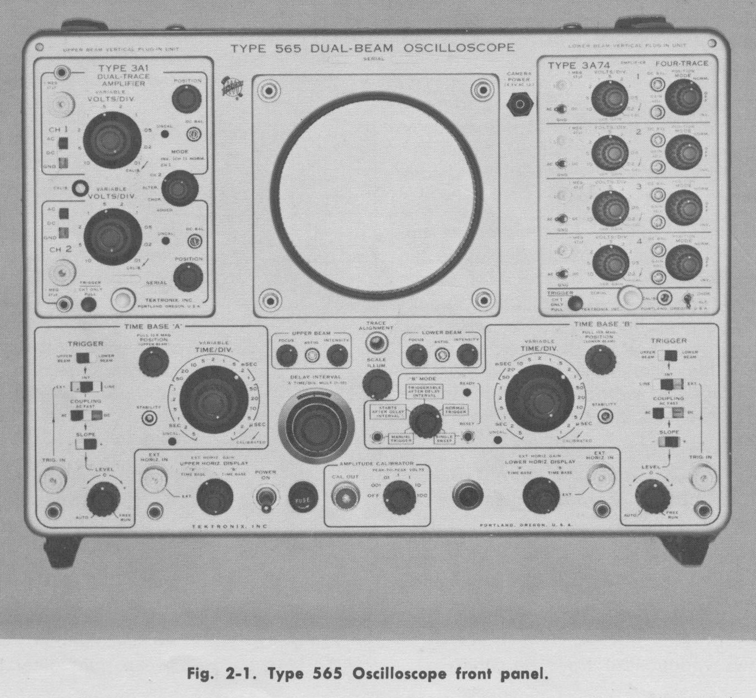
Per ingrandire le immagini cliccare su di esse col tasto destro del mouse e scegliere tra le opzioni.